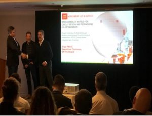
Leti, a research institute of CEA-Tech, and Silvaco Inc., a leading global provider of software, IP and services for designing chips and electronic systems for semiconductor companies, announced during the IEDM 2018 conference a project to create innovative and unified SPICE compact models for the design of advanced circuits using nanowire and nanosheet technologies.
The new predictive and physical compact model under development, Leti-NSP, builds on Leti’s 15 years of model development, including the popular Leti-UTSOI model for FD-SOI technology. The Leti-NSP compact model uses a novel methodology for the calculation of the surface potential, including quantum confinement. The model is able to handle arbitrary cross-section shapes of stacked planar and vertical GAA MOSFETs (circular, square, rectangular). It provides an excellent tool for design exploration of nanowire and nanosheet device architectures.
This three-year collaboration will make the new device models available to designers through SmartSpice, Silvaco’s high-performance parallel SPICE simulator for use by circuit designers. The corresponding model-parameters extraction flow will be implemented in Utmost IV, Silvaco’s database-driven environment for characterizing semiconductor devices, to ensure an accurate fit between simulated and measured device characteristics.
Accuracy of analysis at the nanometer scale is essential for co-optimization of silicon process technology and circuit performance. Besides accurate device characterization and simulation, a complete solution includes TCAD simulation, and 3D parasitic extraction. Silvaco’s partnership with leading research institutions for atomistic TCAD, and its proven in-house extraction solver technology, will provide the most accurate Design Technology Co-Optimization (DTCO) solution for nanometer technologies.
“Over two decades, CEA-Leti and Silvaco have collaborated on design-technology co-optimization, ranging from innovative TCAD simulation to the design of advanced nanoelectronics, and thus expanded and strengthened Silvaco’s suite of tools for designers,” said Emmanuel Sabonnadière, CEA-Leti CEO. “This project continues that partnership, and when these physics-based compact models are made available to designers worldwide, they will be able to evaluate the potential of advanced nanowire-based CMOS technologies under development at CEA-Leti.”
“DTCO, including circuit simulation, is fundamental to the development of electronic devices, and shrinking silicon geometries are placing an even greater premium on accuracy to capture and evaluate all the new physical effects in nanometer design,” said Eric Guichard, vice president of Silvaco’s TCAD Division. “Building on past successes of Leti and Silvaco’s collaboration, this project will provide circuit designers and technologists with powerful, advanced design flows that combine CEA-Leti’s physical, predictive, and easy-to-use models with Silvaco’s high-accuracy EDA tools.”


