


Semiconductor plays a very important role in our lives. It had been the core of electronics industry, the foundation of each and every electronic gadget we use today, in our day-to-day life. The power electronics industry is heading towards the wide bandgap compound semiconductor materials particularly Silicon Carbide and Gallium Nitride from Silicon. SiC has emerged as a strong contender for high voltage markets especially for Electric Vehicles and Solar PV. The other verticals include High Temperature applications viz., Data Centres, Industrial Motor applications, 5G base stations, Smart Agriculture and Irrigation.
India has been the house of many Design and R&D centres for semiconductor manufactures but we have been dependent on other countries for its manufacturing. Establishing a semiconductor fab in India had always been a long journey which is now seems to be cut short on Jan 27th.
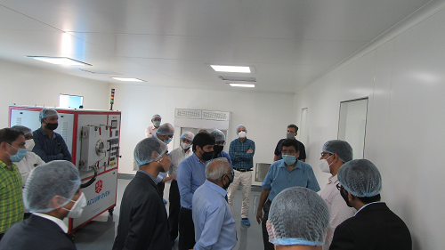
Silicon Power Corporation, founded in 1994, headquartered in Malvern, United States has opened its subsidiary the SiC fabrication unit in Halol (Gujarat) India, bringing lot of opportunities for the Indian Electronics sector. Inaugurated by Mr. Saurabh Gaur, MEITY Joint Secretary, the SiC plant is first of its kind fabrication unit in India opened for the commercial market.
The pandemic effect in major fab countries, shortage of semiconductors and border tensions has fuelled the need of fabrication unit. According to ASSOCHAM India imported about USD 5 billion worth electronic goods” and in 2020, this demand have crossed USD 400 billion. Opening of this new SiC fabrication will not only accelerate India’s objective to create and develop a “Make in India” Electronic devices Industry, but also reduce dependence on imports, especially from China.
Our technical editor, Pratibha Rawat has in-depth conversation with Company’s president Dr. Harshad Mehta on their latest fabrication facility. Below are excerpts:
Previous attempts of opening Fabs in India did not turn out well. Big headlines of investing millions turned out to be failed aspirations. What has inspired you to open SiC fab in India?
This is not our first company in India, we have a small unit named Ruttonsha International Rectifier Ltd which actually has in-house facility for die fabrication, soldering, encapsulation and testing of power components. My roots are in India and firmly support Government make in India mission. We wanted to bring SiC technology to India for supporting electronics manufacturing inspite of importing. Our SiC company will be called Visicon Power and will be a subsidiary of Silicon Power.
“We will not only do wafer fabrication but right from designing to end product every process will be done in India itself. Wafer, packaging and full integration of device which is meant to be true Make in India.”
“This is going to be the first commercial Fab of SiC in India.”
Risk of investment returns, lack of government policies and ecosystem have always pulled the legs of companies. What your intake on this?
Talking about Investments, yes to invest Billions of dollars is a difficult proposition. We are taking smaller steps by investing 20-25 million to get return faster. Working on phases is a good option.
Our Facility is approved under the government’s Production Linked Incentive Scheme (PLI) for large-scale electronics manufacturing. We are also looking forward for expression of interest (EoI) invited by MEITY from companies of setting up/expansion of existing Semiconductor wafer/device fabrication (FAB) facilities in India or acquisition of Semiconductor FABs outside India. Under this we are planning to for GaN another Wide band gap semiconductor in the future.
Building ecosystem is not just few days journey. Having the right policies, fruitful incentives, supply chains developing, all of the ecosystem has to come together to establish a true make in India. This will take time, but we remain committed to this vision.
As you said it is not just a fab but a complete wafer to end product facility. Will it only serve India?
We are building a global organization our focus is not just Indian market but a global market. WE are going to make a true “Make in India” semiconductor company by designing, manufacturing and packaging in the country itself. Our Fab will not only reduce dependency of electronics from outside in India but would also gratify India’s need outside the country.
Tell us about the production and capacity of the facility?
We are starting with 6-inch wafer production line and right now we have focused on minimum capacity needed to build a fab and after it sky is the limit and will be driven my market needs. We have also added clean rooms and as our first initiative will be starting to offer epitaxial layer manufacturing services.
Hope this move will start a new revolution in country. The Indian Government and MEITY are trying hard to establish Fabs by introducing Production Linked Incentive Scheme (PLI) for Large Scale Electronics Manufacturing and inviting expression of interest (EoI) from companies for setting up/expansion of existing Semiconductor wafer/device fabrication (FAB) facilities in India or acquisition of Semiconductor FABs outside India.


