


Silicon carbide transistors are increasingly used in high-voltage power converters as they can meet the stringent requirements regarding size, weight, and/or efficiency of these applications. But why is this technology so fascinating to engineers? The blog will provide some insights.
The outstanding material properties of silicon carbide (SiC) enable the design of fast-switching unipolar devices instead of Insulated Gate Bipolar Transistor (IGBT) switches. Thus, solutions that have only been feasible in the low-voltage world with voltages of 600V and below are now possible at higher voltages as well. The results are increased efficiency, higher switching frequencies, less heat dissipation, and space savings—benefits that, in turn, also reduce the overall system cost.
Infineon Technologies identified this potential almost 30 years ago and established a team of experts in 1992 to develop SiC diodes and transistors for high-power industrial applications. Here is a short and incomplete list of milestones reached since then:
- The world’s first introduction of SiC-based Schottky diodes in 2001
- The first power modules containing SiC devices in 2006
- The release of the current fifth-generation of SiC diodes
- The full switch to the 150mm wafer technology in the Villach Innovation Factory in connection with the premiere of the innovative Trench CoolSiC™ MOSFET in 2017
Metal-oxide-semiconductor field-effect transistors (MOSFETs) have been commonly accepted as the concept of choice when aiming at reliable SiC devices. Initially, junction field effect transistor (JFET) structures seemed the ultimate solution for merging performance and reliability in a SiC transistor. However, with the now established 150mm wafer technology, trench-based SiC MOSFETs have become feasible. This way, the dilemma of double-diffused metal-oxide semiconductors (DMOS) structures of having either performance or high reliability could be solved.
Wide bandgap-based power devices—such as SiC diodes and transistors, or gallium nitride high electron mobility transistors (GaN HEMTs)—are nowadays common elements in the library of power electronics designers. But why? What is so fascinating about silicon carbide in contrast to traditional silicon? What makes SiC components so attractive to design engineers that they use them so frequently in their designs despite their higher costs compared to silicon high-voltage devices? Let’s look at a few reasons.
Low Losses and a High-Breakdown Field Are Key
In power conversion systems, design engineers continuously strive to reduce energy losses during the conversion. Modern systems are based on technologies in which solid-state transistors are switched ON and OFF in combination with passive elements. For the losses related to the transistors used, several aspects are relevant.
- First, design engineers must consider losses in the conducting phase. In MOSFETs these are defined by a classical resistance. In IGBTs, it’s a fixed conduction loss determinator in the form of a knee voltage (Vce_sat) and additionally a differential resistance of the output characteristic. The losses in the blocking phase can usually be neglected.
- Second, design engineers should consider that there is always a transition phase between the ON and OFF state during switching (Figure 1). The related losses are defined mostly by the device capacitances. In IGBTs, further contributions are in place due to the minority carrier dynamics (turn-on peak, tail current).
Based on these considerations, you would expect that the device of choice is always a MOSFET. However, especially for high voltages, the resistance of silicon MOSFETs becomes so high that the total loss balance is inferior to that of the IGBTs, as these can use charge modulation by minority carriers to lower the resistance on conduction mode.
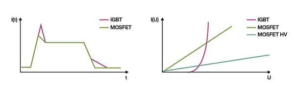
Figure 1: The figure shows a graphical comparison of the switching process and the static I-V behavior. (Source: Infineon Technologies)
The situation changes when wide bandgap semiconductors are considered. Figure 2 summarizes the most important physical properties of SiC and GaN versus silicon. The direct correlation between the bandgap and the critical electric field of a semiconductor is significant. With SiC, it is about 10 times higher as compared to silicon.
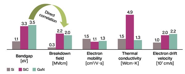
Figure 2: The image highlights critical physical properties of SiC and GaN versus silicon. (Source: Infineon Technologies)
With this feature, the design of high-voltage components is different. Figure 3 shows the impact, using the example of a 5kV semiconductor device. In the case of silicon, semiconductor designers are forced to use a relatively thick active zone because of the moderate internal breakdown field. In addition, only a few dopants can be incorporated in the active area, thus resulting in a high series resistance (as indicated in Figure 1).
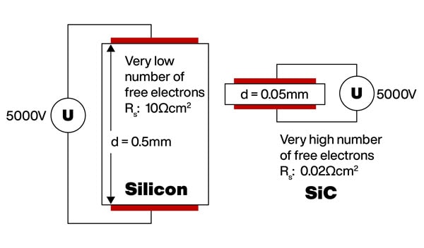
Figure 3: SiC allows for thinner semiconductor active zones. (Source: Infineon Technologies)
With 10 times higher breakdown field in SiC, the active zone can be made much thinner. At the same time, many more free carriers can be incorporated, and thus, a substantially higher conductivity can be achieved. It can be said that in the case of silicon carbide, the transition between fast-switching unipolar devices such as MOSFETs or Schottky diodes, and the slower bipolar structures such as IGBTs and p-n diodes, has now shifted to much higher blocking voltages (Figure 4).
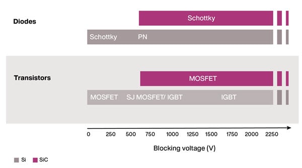
Figure 4: SiC offers higher blocking voltages than traditional silicon. (Source: Infineon Technologies)
Or vice versa: what was possible with silicon in the low-voltage range around 50V is with SiC feasible for 1200V devices.
Conclusion
Advances in WBG technology and silicon carbide’s superior material properties enable these devices to operate with faster switching, low switching losses, and a thinner active zone, resulting in designs with increased efficiency, higher switching frequencies, and better space savings. As a result, SiC MOSFETs are becoming the preferred option over traditional silicon for power conversion applications.
The source of the blog is Mouser Electronics
https://www.mouser.com/blog/what-are-benefits-and-use-cases-of-sic-mosfets


