


Abstract
O-RAN was created as a catalyst to transform the wireless community, to enable new channels of wireless equipment, and to enable innovation to fulfill the promises made by 3GPP about 5G.1 To be successful and cost-effective, open sources of radio equipment and optimized 5G technology devices must be available. This article will review one of those solutions for designing and building a power efficient solution.
What Are the 5G Challenges?
There are several techniques that radio and network engineers are using to achieve these goals. In addition to moving data services to the edge of the network, utilization of both massive MIMO and small cell technology aids in increasing both capacity and throughput. Massive MIMO technology utilizes numerous radios in an array to achieve not only capacity but also coverage for a central location. Like its predecessor the macrocell, a massive MIMO radio would provide relatively broad coverage around that location. However, massive MIMO radios are placed at higher frequencies, typically 2.6 GHz and above, that do not penetrate buildings very well. To service indoor locations and other difficult to reach outdoor areas, small cells will be utilized. Given the number of indoor and outdoor locations ranging from households to enterprise installations to commercial shopping areas and even arenas, small cell utilization will be vital to the success of 5G. Given the vast numbers of small cells and diversity of deployments required in a network, they must be inexpensive to install and operate; this will be a key enabler of 5G.
What Technologies Are Available?
Over the last few years, multiple technologies have evolved in a direction that enables solutions for 5G. Firstly, from a baseband perspective, Moore’s law continues to not only reduce the cost of silicon per gate but enable more complex functionality to be integrated into radio technology. It is now possible to integrate many of the control algorithms required directly into the radio, including functionality like digital predistortion (DPD). Many other possibilities exist as new generations of radios become available.
Second, industry alliances like O-RAN2 are working across the wireless industry to enable economies of scale not only to reduce cost, but to improve supply chain security and to offer new ways to monetize these wireless networks. Specifically, “the O-RAN Alliance was founded by operators to clearly define requirements and help build a supply chain eco-system to realize [its] objectives. To accomplish these objectives, the O-RAN Alliance’s work will embody” the principles of openness and intelligence.3 As such, their activities focus on defining the physical interfaces specified by 3GPP so that they can be standardized and implemented across the industry as interoperable white box solutions. Additionally, O-RAN also defines the hardware requirements and provides reference designs for the O-CU, O-DU, and O-RU (Open Centralized Unit, Open Distributed Unit, and Open Radio Unit, respectively—as defined by O-RAN). Together these will enable standardization of fronthaul and baseband processors to further reduce solution cost. Together with other integrated 5G devices like integrated radios, these can serve to define what small cells are to become as well as enable the implementation of those standards. The work of these bodies is a critical step.
Third, radio technology has rapidly evolved in the last few years. High performance radios are now available in several formats capable of meeting the required performance standards demanded by 3GPP in 38.104 and related documents.1 These radios are highly integrated and include not only the analog and RF components but critical algorithms like DPD and crest factor reduction (CFR). While these radios are built on fine-line CMOS, other evolutions have taken place in the RF front ends where low cost RF processes (SiGe, SOI, GaN, GaAs, etc.) are turning out highly integrated LNAs and high power, high performance PAs that can meet the challenges these standards demand.
Finally, highly integrated and efficient power solutions—including power over Ethernet (PoE), standard power device, supervisory and monitoring, and protection solutions—are available that can provide compact power delivery. These solutions offer very high efficiency and very low noise in the radio environment and include options that provide protection of key devices like power amplifiers.
Together, these technologies are enabling low cost, high performance small cell platforms that can effectively be deployed throughout an operator’s network for both low and high power systems.
System Overview
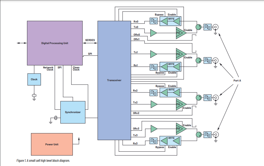
Figure 1 shows a typical 4T4R (four transmitters and four receivers) 5G small cell block diagram. There are many permutations possible, including 2T2R and a range of power classes from 24 dBm and higher. This figure will be the basis for the remainder of the discussion, focusing on 5G technology devices that are easily scaled for band and power level variations within the O-RU.
Key Radio Elements
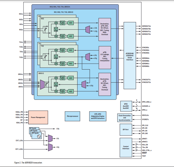
Over the last decade, the integrated transceiver has matured into a high performance platform. The ADI RadioVerse™ family includes a wide range of integrated transceivers that support up to 200 MHz of occupied bandwidth, integrating advanced features like DPD. Together, this family of products not only meets the needs of 5G technology devices, but also continues to support LTE and multicarrier GSM RF requirements. While new generations of these devices are always in development, one of the latest is shown in Figure 2, the ADRV9029, a 4T4R configuration. Other products are available that include devices with and without integrated DPD and other configurations including 2T2R.
Each RadioVerse device includes everything required to construct a complete radio except for the LNA and PA. This includes all functionality for transmit and receive, synthesizers, and clocking. It also includes the state machine and VGA required to run the AGC and gain control amplifier. While the RadioVerse products are all broadband up to 6 GHz, LNAs and PAs are not and must be specified by band or frequency range. Therefore, to complete the radio design a suitable LNA and PA must be paired with the RadioVerse IC. The following sections will describe the signal chain for both the receive and transmit for a 5G NR small cell design and give some insight into selection of those devices.
Example Receiver Signal Chain
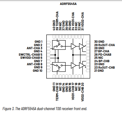
When the ADRV9029 is combined with the ADRF5545A, as shown in Figure 3, a 2-chip receiver is easily constructed. The ADRF5515 is pin compatible and can also be used. Combined with only a few other passive components, this can form a very compact, high performance receiver design as shown in the signal chain in Figure 4. The key advantage to this architecture is the high level of integration possible, which leads not only to a very low cost implementation but also to the lowest power dissipation possible.4
The architecture of the RadioVerse family leads to the elimination of many elements typically associated with a classic receiver design including some of the RF amplification, filtering, and integration of much of the remaining radio functionality, including channel filters (analog and digital) and baseband amplifiers. These are typically some of the largest and highest power devices in the system, which results in significant savings over other architectures like direct RF sampling.
As shown in Figure 4, the small cell receiver lineup consists of a circulator (for TDD applications), ADRF5545A, SAW/BAW (surface acoustic wave/bulk acoustic wave) or monoblock filter, balun, and transceiver. Additional amplifiers or VGAs are not required given the good noise performance and low input IP1dB of the ADRV9029 and other members of the RadioVerse family. Using this signal chain, it is possible to support noise figures as low as 2 dB for the complete system from the antenna to bits. While this design includes an integrated RF front-end module (FEM), many designs will still benefit from a discrete design not represented here. The integrated FEM trades off integration for slightly increased filter requirements in the antenna filter but still offers a compelling design for many highly integrated solutions such as massive MIMO and other TDD deployments. Typically, discrete front ends are used for FDD designs.
Assuming a loss prior to the LNA of about 0.5 dB, and if the loss of the band filter is 1 dB, given the data sheet specs of the two active devices, the nominal NF for the complete receiver signal chain should be about 2 dB. Assuming a 0 dB signal-to-noise-and-distortion ratio consistent with MCS-4, the reference sensitivity will be about –104.3 dBm for a G-FR1-A1-1 5G carrier (~5 MHz). This should be more than adequate to meet even the wide area conducted requirements shown in section 7.2.2 of 38.104 with room for margin, and much more than enough for a local area/small cell design that requires –93.7 dBm for this condition as summarized in Table 1. Some low performance small cell applications may be able to utilize a single stage LNA such as GRF2093 followed by a SAW filter.
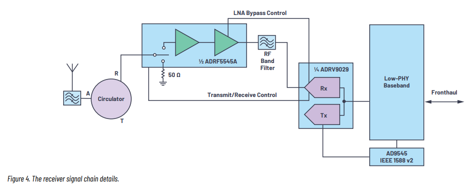
Table 1. 38.104 Receiver Classifications
| Wide Area (dBm) | Medium Range (dBm) | Local Area (dBm) | |
| 5 MHz BW/15 kHz | –101.7 | –96.7 | –93.7 |
| 20 MHz BW/15 kHz | –95.3 | –90.3 | –87.3 |
| 50 MHz BW/30 kHz | –95.6 | –90.6 | –87.6 |
| 100 MHz BW/30 kHz | –95.6 | –90.6 | –87.6 |
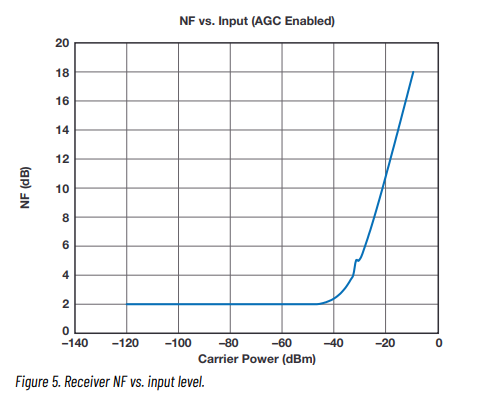
Additionally, 38.104 section 7.4.1 requires that under –52 dBm (wide area) ACS blocking that the receiver not desense more than 6 dB. Based on the NF vs. input level shown in Figure 5, very little additional noise occurs at –52 dBm than at lower levels. In fact, the noise floor doesn’t tilt upward until just after –40 dBm, which is ideal for the local area ACS that requires
–44 dBm tolerance.
General blocking requirements (7.4.2) call for an aggressor of –35 dBm (local area) to be applied to the receiver within the band of interest at an offset of ±7.5 MHz with no more than 6 dB desense allowed. From Figure 5 showing the Analog Devices signal chain performance, only about 0.9 dB desense has occurred. Narrow-band blocking is a slightly lower power CW-like stimulus but is not a problem either.
Perhaps a more interesting challenge will be the out-of-band blocking from section 7.5.2. Here a signal of –15 dBm is passed to the antenna input. For a small cell with less than 200 MHz, the closest this signal can be to the band edge is 20 MHz. The test requires a sweep from 1 MHz up to 12.75 GHz, excluding the band within 20 MHz of the operational frequency. There are several things working to the signal chain’s advantage here. First, the circulator has a finite bandwidth and will reject many out-of-band signals, but close in it is not a big contributor. Second, the filter shown after the ADRF5545A will provide some filtering—typically, 20 MHz out-of-band ~20 dB rejection is reasonable. Finally, one of the unique and most useful features of ADI’s transceiver family, inherent to the transceiver architecture, is built-in out-of-band rejection. In Figure 20 from Analog Devices’ application note AN-1354, inherent out-of-band rejection is demonstrated as an increasing signal level to desense the receiver. In this application note, sweeping frequency in either direction around the pass band shows that a larger signal is tolerated for the same level of desense. In the application note, we see that near the band edge about 10 dB is possible for 6 dB desense. Beyond this the integrated filter rolls off significantly out-of-band signals, which do not alias back in-band and are largely attenuated both by on-chip and external filtering.
Together these blocks filter the –15 dBm out-of-band aggressor to approximately –40 dBm to –45 dBm up to the 20 MHz exclusion band. Further out, even greater rejection would be assumed. At this level, Figure 5 shows very little desense would be expected.
Perhaps the bigger problem would be the linearity of the front-end module. At this level, a significant IM3 product could be anticipated. Depending on the actual FEM selected, it may be desirable to move the band selection filter before the second LNA to protect it from out-of-band signals, which typically produce large IM products. It is not possible to place a filter between the stages on this these types of FEMs, so an alternate option is implemented.
To aid in limiting the impact of intermods under large out-of-band blockers, a typical FEM includes second stage bypass switches to reduce gain and to protect the second stage from being driven into nonlinearity, as shown in Figure 3. Toggling the LNA gain reduces the signal chain SNR by 1 dB but aids in preserving the overall dynamic range by limiting intermodulation distortion caused by these large blockers, more than offsetting the loss of noise performance. Overall, this would result in a worst-case NF of about 5.7 dB, which is still within the local area (small cell) footprint requirement on reference sensitivity. Any remaining filter requirements are supplied by an antenna filter, and rejection can be determined based on the low gain compression point and IP3 of the receiver FEM.
Example Transmitter Signal Chain
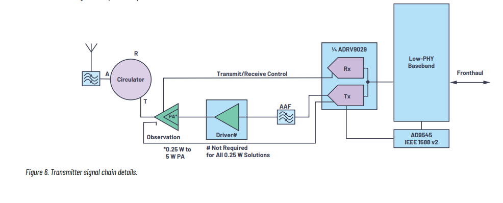
When the ADRV9029 is combined with a suitable RF drive amplifier, or RFVGA (visit analog.com/rf for more options), and a suitable PA, a compact indoor picocell, outdoor picocell, or outdoor microcell5 are easily constructed. With only a few other passive components, these 5G technology devices can be combined to form a very compact and efficient transmitter design, as shown in the signal chain in Figure 6. The key advantage to this architecture is the high level of integration possible, which leads not only to a very low cost implementation but also to the lowest power dissipation possible by utilizing the integrated DPD functionality available on select ADI transceivers.
As shown in Figure 6, the small cell transmitter lineup consists of a circulator, PA, filter, and transceiver. Additionally, the circuit includes a coupler on the output of the PA that is used to monitor the output distortion (and can also be used to monitor the VSWR of the antenna as well as forward power) and can be used with DPD to improve the operational efficiency of the transmit function and improve spurious performance. While an external DPD can be used, select ADI transceivers include fully integrated DPD, which operate on 350 mW or less incremental power depending on the amount of correction a given PA requires. Lower power PAs will require less correction and therefore less power consumed by the DPD. In addition, the integrated DPD reduces the number of SERDES lanes by one-half to the external baseband chip as the observation receiver SERDES lanes are eliminated completely and the transmitter payload is reduced, given the bandwidth expansion for DPD is handled completely within the transceiver. An equivalent DPD in an FPGA typically has 10× higher power and is not effective or power efficient for low power small cells and massive MIMO. However, by integrating the DPD into the transceiver, the very low power and small cost effectively enable DPD to be used even for low power small cells and thus reap the benefit in efficiency and improved transmit linearity without a heavy external computation burden.
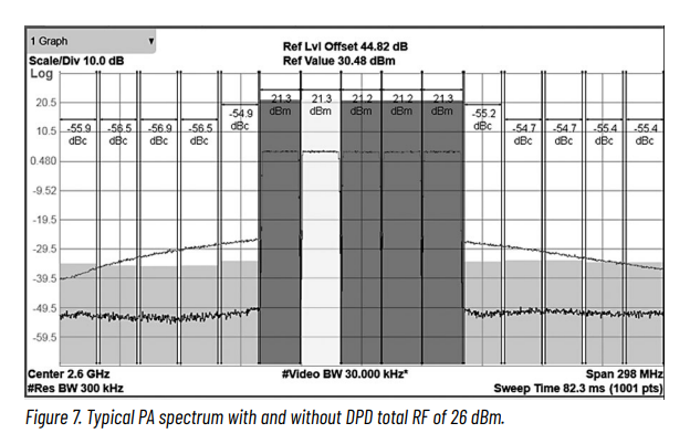
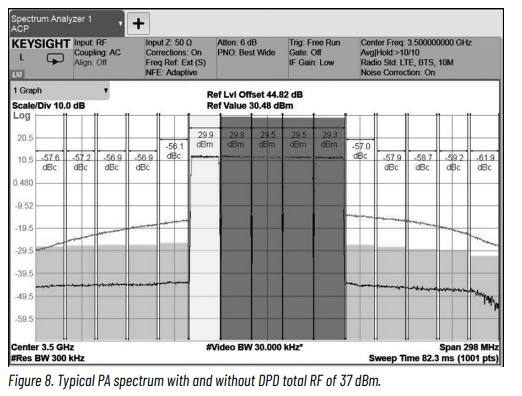
Figure 7 and Figure 8 show examples of ADI’s DPD working in low and medium power small cell applications. The stimulus shown is for five adjacent 20 MHz LTE carriers with a total of 100 MHz. Typically, LTE requires a minimum of 45 dB ACLR with most deployments expected to get more than this. ADI runs an ongoing testing lab always reviewing new PAs of all power classes. Check the Power Amplifier Test Report, or consult the factory for the latest details on available DPD technology from ADI as well as a list of the latest qualified PAs.
How Does It All Come Together?
Figure 9 shows the full signal chain including some of the required control signals. For power efficiency, the circuit includes transmit and receive signaling to enable and disable the amplifiers during their respective cycles for TDD. Similarly, this could be used with FDD to power-off during unused slots to save power then as well. An LNA switch is also required to change the input switch on the LNA to shunt any returned transmit power to a termination instead of the core amplifier input. These various signals can be generated and orchestrated by the ASIC, FPGA, or transceiver.
The receiver signal chain includes a function that correspondingly changes the digital data stream to account for the reduced analog gain, preserving the absolute signal level as it is passed to the low-PHY and then on to the remainder of the baseband downstream.
The application shown here is for single band. While the transceiver is broadband and covers all frequencies up to 6 GHz, not all devices in the design do. Devices like the LNA and PA are typically banded and require selection based on band supported. Typically, these devices are available in pin-compatible options to cover all common bands below 6 GHz and are easy to swap out. This enables support for all the popular TDD and FDD bands, including those for 5G and those proposed for O-RAN.
Clock Tree
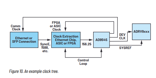
Depending on the configuration, several different clock configurations are possible. If precise timing alignment is required, then a 2-stage clock synthesis will be required. The first stage will require linkage to the baseband by way of an ASIC, FPGA, or controller to properly time and align the radio digitization. This application will require processing of the precision time protocol (PTP) information provided by way of the fronthaul or by a local GPS receiver. This will ensure that the radio and baseband processor know precisely when radio frames should be processed.
The AD9545 family is ideally suited for precisely adjusting the frequency, phase, and time of the main clock to the radio. It has the benefit that it can be configured to operate temporarily without a reference and maintain accuracy in the case of a faulty or intermittent reference clock when coupled with a TCXO (temperature compensated crystal oscillator) or OCXO (oven controlled crystal oscillator).
For configurations that do not require the precise timing alignment or as the second stage of those that do, a clock distribution device is required. The purpose of the distribution device is to generate the range of clocks throughout the radio. This includes those required for JESD, eCPRI, Ethernet, SFP, and other key signals throughout the radio. The AD9528 provides low jitter clocks to a total of up to 14 different rates, including support for JESD204B/JESD204C device clock and SYSREF signaling.
A 2-stage clock block diagram is shown in Figure 10. For applications that don’t require precise timing alignment, the AD9545 can be eliminated or bypassed and only the AD9528 would be used. The input clock to the system comes from basic network timing and is recovered by the baseband and network functionality of either the Ethernet function block or within the FPGA, depending on the exact architecture. Many alternate configurations are possible depending on the specific requirements of the radio with only a representation shown here.
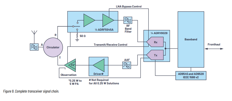
Figure 9. Complete transceiver signal chain.
Power
Rolling up the total power dissipation is determined by many factors. Among these factors include the FPGA selected and the functions implemented, the transceiver selected and options enabled, the clock tree required, and the RF power generated.
A typical mid-range FPGA SoC implementing the O-RAN CUS- and M-plane processing, along with synchronization with IEEE 1588 v2 PTP stack, will consume around 15 W. The typical ADRV9029 transceiver will dissipate between 5 W and 8 W, depending on TDD or FDD configuration along with the range of DFE functionality enabled. To this the clocking power, receiver power, transmitter power, as well as miscellaneous powers must be added. Table 2 shows an example rollup of the total power for the system exclusive of the transmitter chain, which varies greatly with power output class.
Rolling up the power dissipation for the radio, total dissipation for a 70:30 duty cycle for Tx:Rx shows 26 W to 29 W, depending on the exact radio configuration excluding power associated with the PA. Table 3 shows a few examples of PA dissipation. Because PAs operate largely in the linear range of the transistors in some variation of a class AB, their efficiency could be anywhere between 20% and 50%. This is where the value of integrated DPD is a big benefit. Even for small bandwidth, low power PAs, a few dozen mW of DPD dissipation is more than offset by the improvement in efficiency of the PA.
Table 2. Budgetary Power Dissipation
| Device | # Required | TDD 70:30 Typical Dissipation (4T4R) |
| Mid-range FPGA SoC | 1 | ~15 W |
| ADRV9xxx | 1 | ~5 W |
| ADRF5545A | 2 | 0.6 W |
| AD9545 | 1 | 0.7 W |
| AD9528 | 1 | 1.4 W |
| PA drive amp | 4 | 1.2 W |
| Misc. | 1 | 2 W |
| Total | 14 | 26 W to 29 W |
Table 3. Transmit Power Dissipation
| Device | # Required | TDD 70:30 Typical Dissipation (4T4R) |
| PA (+24 dBm/antenna) | 4 | ~2.5 W |
| PA (+37 dBm/antenna) | 4 | ~47 W |
For a low power small cell, adding in about 2.5 W of additional power brings the total dissipation to about 30 W, which is comfortable for a passively cooled indoor small cell powered by a PoE solution.
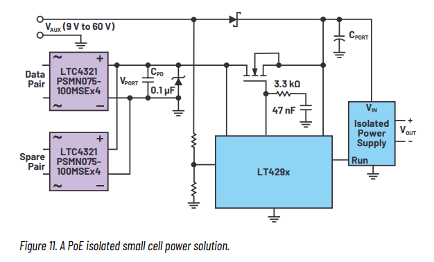
One potential PoE solution is outlined in Figure 11. This solution includes the LT4321 bridge controller that allows MOS transistors to be used as ideal diodes instead of rectifiers, the advantage of which is much improved efficiency. This is followed by the LT4295, an 802.3bt compliant PD device. This can then be followed by appropriate local regulators to fulfill the requirements shown in the previous table, providing up to 90+ W as required.
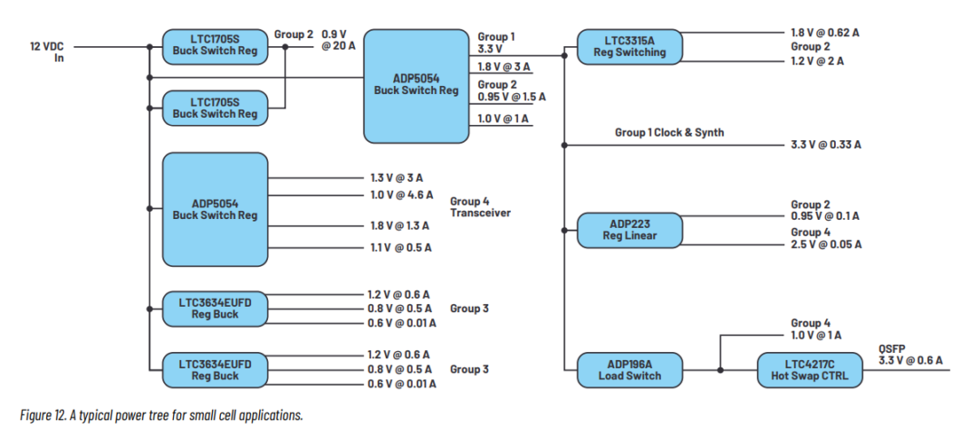
Beyond the PoE conversion devices, many other devices are available in support of a small cell reference design. These include cornerstone devices like the ADP5054 family, which is specifically designed to power ADI transceivers as well as many other buck converters and lower noise LDO regulators, as shown in Figure 12.
Options
One of the great things about this radio architecture is the flexibility that it affords in terms of meeting a range of market requirements. This architecture is optimized for a range of applications including both FDD and TDD. It is equally capable of performance in low, mid, and high band and is well suited for small cell through massive MIMO platforms. Many different trade-offs can be made in both the transmitter and receiver circuits to optimize for cost, size, weight, and power. While this introduction focused on higher performance and integration, it is possible to make some simple trade-offs in favor of cost with slightly different selections.
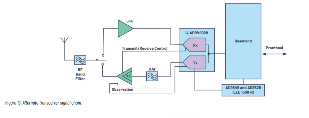
For example, some low power PAs do not require a drive amplifier and therefore may not be required. Because the RF power is low for many small cell applications, the circulator may be replaced by a simple TR switch. Finally, if only local area performance is required the dual stage LNA may be replaced by a simple single stage LNA. The result is a lower cost option still providing good radio performance. An example of this is shown in Figure 13. Many other permutations are available to suit a wide range of possibilities across a wide range of frequency and power options.
Conclusion
The 5G technology devices reviewed here are available for communications applications and enable low cost implementations suitable for 5G development, especially those implementing O-RAN O-RU solutions. These include devices from the RadioVerse family as well as RF amplifiers, clock recovery/synchronization, and power over Ethernet/point of load regulation. Together this highly integrated set of devices is ready for implementation of 5G small cell, macrocell, microcell, and massive MIMO applications.
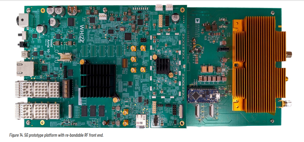
When combined with a suitable PHY and software provided in an FPGA, eASIC, or ASIC, a complete O-RU solution may be developed, as shown in Figure 14. This solution was developed with partners at Intel®, Comcores, and Whizz Systems. These solutions meet not only the required RF characteristics but also the cost and power budgets required to enable deployment of low cost, high performance O-RAN platforms.


