


Global warming, scarcity of natural resources and pollution are environmental issues which are becoming increasingly important worldwide. Two wheeler Electric mobility (e-mobility) represents an effective solution to many of the problems. It offers a green alternative to vehicles based on traditional internal combustion engines. India is the second largest Producer and manufacturer of two-wheelers in the world. It stands next to Japan and China in terms of the number of two-wheelers produced and domestic sales. Indian two-wheeler industry has embraced the new concept of electric mobility that are very popular mode of personal transport.
What is a DC to DC converter? A DC-to-DC converter is an electronic circuit that converts a source of direct current (DC) from one voltage level to another. It is a type of electric power converter. The different configurations of EV power supply show that at least one DC/DC converter is necessary to interface the Battery to the DC-link. This electric circuit converts a source of direct current (DC) from one voltage level to another, by storing the input energy temporarily and then releasing that energy to the output at a different voltage. The storage may be in either magnetic field storage components (inductors, transformers) or electric field storage components (capacitors). The amount of power flow between the input and the output can be controlled by adjusting the duty cycle (ratio of on/off time of the switch). Usually, this is done to control the output voltage, the input current, the output current, or to maintain a constant power.The main requirement of this converter is to power up the auxiliary load like E-horn , LED lights and other peripheral functions.
Industry Challenges :
It is vital aspect of battery powered Vehicles that the use of DC-DC converter is inevitable to achieve to calm the range & anxitey of user. The DC-DC converters in the industries are known to produce high frequency radio emissions, commonly termed as RE. ST as a technology provider has enhanced the performance of discrete power devices alongwith new generation of control DC-DC integrated Controller. ST’s device makes use of high capability gate drivers to operate MOSFETs at high switching speeds that helps to reduce both the size of energy storage components and radiated emissions.
ST’s Offering :
ST has come up with a versatile DC-DC Synchronous controller with operating in rage of 6V to 75V making it usable in wide range of application. The reduced peripheral component around the device makes the development process easy while reducing the size of PCB. The new device L3751 synchronous buck controller features extreme voltage conversion ratio over switching frequency range (100 kHz – 1 MHz) thanks to 40 nsec minimum conduction time. This controller implements pulse skipping mode that maximizes the efficiency at light-load giving controlled output voltage ripple. The forced PWM (FPWM) over the load range makes the switching frequency constant and minimizes the output voltage ripple. An embedded gate driver minimizes the number of external components and it is designed for standard VTH MOSFET. Embedded protections–output overcurrent, input voltage UVLO, internal voltage monitoring, thermal shutdown – feature controlled and safe operation for critical aplications like two wheeler electric mobility.
Typical Schematic and block Diagram:
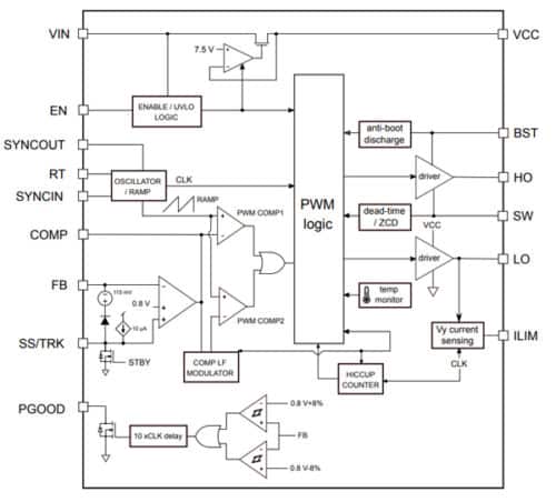
Functional Description:
The L3751 device is a native buck controller based on constant frequency voltage mode architecture.
The output voltage VOUT, sensed by the feedback pin (FB), is compared to an internal reference (0.8 V) providing an error signal on the COMP pin. The comparison between the COMP voltage level and the internal programmable frequency sawtooth ramp, controls the activation time of the external power switches. The main internal blocks are shown in the block diagram in Figure 2 and can be summarized as follows:
• The voltage regulator to supply the internal circuitry and provide a fixed internal reference. This block also implements a voltage monitor circuitry (UVLO) that checks the input and internal voltages
• The embedded external N-channel MOSFET drivers and the bootstrap capacitor circuitry to supply the high-side driver
• The embedded circuitry that generates the sawtooth ramp to modulate the duty cycle based on the internal programmable oscillator or the input synchronization signal. The input voltage feedforward is implemented for improved line transient response
• The voltage mode error amplifier
• The PWM comparators and the relative analog and digital circuitry necessary to drive the internal MOSFET drivers
• The soft-start circuitry to limit inrush current during the start-up phase and the reference clamper • The adjustable senseless or precise valley current limit sensing block and hiccup circuitry to handle overload and short-circuit conditions
• The thermal shutdown circuitry to prevent thermal runaway
• The output voltage monitor circuitry which releases the PGOOD signal if the sensed output voltage is above 87% of the target value.
The specific feature of Diode Emulation Mode (DEM) enhances the efficiency of application at light loads.
The DEM mode operates in DCM and pulse skipping at light load, so maximizes the efficiency in these application conditions minimizing the conversion losses with controlled output voltage ripple. The forced PWM (FPWM) over the load range makes the switching frequency constant and minimizes the output voltage ripple, suggested for low noise application like sensors or analog circuitry supply.
Solution offering:
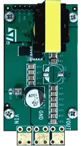
The reference solution as shown in Figure 3 is for DC-DC Converter for Input voltage specifications of 36- 72VDC and Output Voltage of 12VDC and 10A:
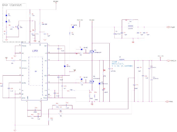
Circuit description:
The input stage comprises of bulk capacitors filter stage in PI network(C4, C5 and L1) to mitigate high frequency emissions caused by high frequency operation. The input DC bus voltage is supplied to VIN pin of device(Pin 20) with serial resistance in path. This is the input voltage to the internal circuitry of controller and to provide voltage to internal LDO to have Vcc output of 7.5Vwhich also powers the internal the embedded gate driver stage. A small MLCC capacitor needs to be connected to pin 20. The enable pin (Pin 1) is biased with voltage divider network from input voltage in order to enable the controller at 40V to avoid deep discharge of batteries. As soon as the EN/UVLO pin voltage exceeds the 1.2 V typical, the soft start phase takes and voltage at SS/TRK ramps up and devices starts. For operation with minimum 40V input voltage operation, the resistors R1 and R6 are selected as 100K and 4.7K respectively. For unconditional stability of control loop and make it independent of types of capacitors the type –III compensator has been implemented, providing us two zeros and three poles. This scheme ensures enough phase margin for improved step load performance.
Performance & Test Results
The board has been tested at various load conditions and the efficiency and performance results have been observed.
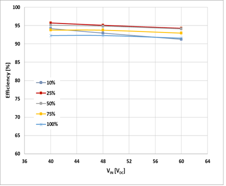
Figure 5: Efficiency @ Vin & load variations
Summary:
The two-wheeler market is growing fast in India. Lot of factors are helping for the growth like Indian Government giving subsidy for Electric Vehicle, petrol pricing increasing, tax rebate from govt for buying of electric vehicle and infrastructure improving helps to accelerate the growth of EV. In this context we can see that new technological development like highly efficient DC-DC Converter helps to have better performance with smaller and efficient solution. The present solution which is developed is catering to the two-wheeler market, but the same switching converter can be used for 3W market where we can target output current level of 30A.


