


Nordson TEST & INSPECTION announced plans to exhibit at SEMICON West 2025, scheduled to take place October 7-9th at the Phoenix Convention Center in Arizona. Visitors to booth 5745 will have the opportunity to see demonstrations of Nordson’s WaferSense semiconductor sensors, Quadra Pro Manual X-Ray System (MXI), Gen 7 Acoustic Micro Imaging (AMI) system and 4800 Integra Bond Tester.

Nordson will be unveiling for the first time in the US, the Auto Centering System (ACS), which is an extension of the wireless, WaferSense sensor portfolio designed for capturing and analyzing real-time data for effective semiconductor tool set-up and maintenance. The wafer-shaped ACS “sees” inside equipment to capture dimensional offset data (x,y and z) to quickly center wafer transfer positions.
The recently launched next-generation Auto Gapping Sensor (AGS2) will also be demonstrated. The AGS2 speeds non-contact gap measurements and parallelism adjustments under vacuum, improving uniformity, tool availability and repeatability in a thinner and lighter form factor.
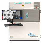
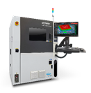
Setting a new industry benchmark for 3D/2D manual inspection in back-end semiconductor applications, the Quadra 7 Pro MXI system revolutionizes the inspection experience with its Onyx detector technology. This advancement ensures exceptional image clarity and elevated levels of precision and efficiency. The Dual Mode Quadra NT4 tube provides unprecedented flexibility. This innovative technology offers both brightness and resolution modes, enabling operators to seamlessly transition between them according to specific application requirements. This ensures optimal results for a wide range of semiconductor inspection needs.
The Gen7 AMI system powered by C-SAM technology, provides fast and highly accurate inspection for detecting delamination and voiding with the most sophisticated microscope. Ideal for lab analysis and specialized high-resolution applications.
Additional inspection and metrology systems & software featured at the show include the following:
Mid-End Semiconductor Solutions
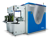
The SpinSAM Acoustic Micro Imaging Inspection (AMI) system sets a new benchmark in the industry with its high throughput and superior sensitivity, enabling precise defect detection for Wafer-Level and Advanced Packaging applications including bonded wafers, Chip-on-Wafer, stacked wafers, MEMS, and over-molded wafers. Using an innovative spin-scanning method, the system scans up to four 300mm wafers simultaneously, achieving an impressive speed of 41 wafers per hour. This breakthrough scanning capability, combined with best-in-class defect capture and image quality, enhances both productivity and accuracy in semiconductor inspection. It is Designed for 100% inspection, as well as edge scanning that targets defect prone areas, optimizing data acquisition where it is needed most.
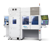
The XM8000 Automated X-Ray Metrology (AXM) system is powered by the QuadraNT tube and detector capable of 2D, 2.5D and 3D measurements of micron scale features with superior resolution. The system is designed for high-throughput metrology and defect review for optically hidden features, including voiding, fill levels, overlay and critical dimensions in Wafer-Level, Panel-Level and Advanced Packaging applications such as CoWoS, TSVs, 2.5 and 3D IC packaging and wafer bumps.
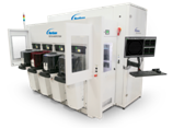
The 4800 INTEGRA Plus is the next generation automated bond test solution designed to meet the dynamic wafer-level packing environment. With its new motion, vision, and wafer handling system complemented by the high-throughput Paragon software, the system offers best-in-class micro bump and trace bond testing on chip-on-wafer, stacked wafer, and molded wafer applications. The system demonstrates unmatched precision, hands-free, and fully traceable bond testing capability for both 200 and 300mm wafers enabled by a smart load port and wafer chuck, and Matrix Map software.
Back-End Semiconductor Solutions
The advanced SQ7000™+ Multi-Function system for AOI, SPI and CMM is designed to address next-generation applications such as advanced packaging, socket metrology, and memory among other high-end applications. This cutting-edge technology enables highly accurate, high-speed inspection and metrology, with an even higher resolution Multi-Reflection Suppression (MRS) sensor that eliminates reflection-based distortions common with shiny and specular surfaces. The SQ7000+ inspects for defects, and measures critical parameters in seconds with a comprehensive coordinate measurement software suite.
The SQ3000 M2 Inspection and Metrology system, designed for micro-electronics applications including wire bonds, provides superior performance with unparalleled accuracy and resolution. Powered by Focus Variation Metrology (FVM) technology and high resolution telecentric optics, the system provides exceptional defect coverage and metrology capabilities.
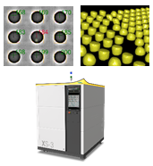
Dynamic Planar CT is the next-generation of3D Planar X-Ray inspection software for our Automated X-Ray Inspection (AXI) systems that reveals incredible details, superior data quality, and clear layer separation, powered by a new 3D reconstruction algorithm. Dynamic Planar CT is ideal for any 3D electronics inspection application, but excels in the semiconductor market for inspection of flip chip micro bumps. Dynamic Planar CT will be demonstrated on Nordson’s XS-3 AXI system. The performance is significantly advanced providing a larger field of view and up to 2× faster image acquisition than classical Planar CT. These speed enhancements yield faster cycle times and greater throughput, while also crucially reducing sample radiation dose.
Advanced ML, DL and AI
Nordson Test & Inspection is at the forefront, advancing Machine Learning (ML), Deep Learning (DL) and Artificial Intelligence (AI) all under the Nordson Intelligence ecosystem. The latest advancement in the ecosystem is Nordson Sight, a complete SPC solution offering full-fledged machine-level to factory-level SPC capability, historical analysis and reporting tools across technology platforms. Nordson Sight provides complete traceability for effective process verification and control, to improve yields and processes. Effectively monitor how well manufacturing processes are running with comprehensive yield analysis charts, coupled with defect analysis tools that enable quick diagnostics and corrective action.
Visit Nordson Test & Inspection at booth 5745 to experience the future of semiconductor inspection and metrology technology that improves yields, processes, throughput and productivity.
For more information, visit www.nordson.com/testinspect.


