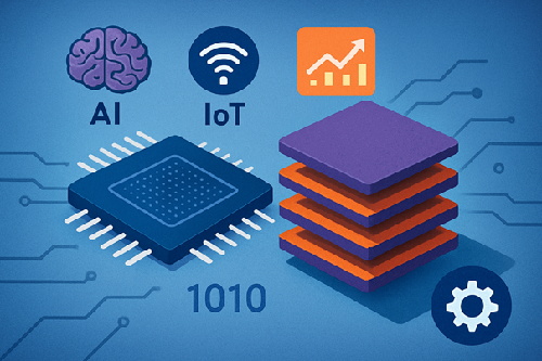
Semiconductor landscape is changing drastically. The old one-size-fits-all chip architectures that have been the mainstay of digital innovations for generations are now finding it hard to comply with the performance, energy-saving, and scalability requirements brought about by new technologies like artificial intelligence (AI), Internet of Things (IoT), and high-performance computing (HPC).
Faced with the increased intelligence of devices and the exponential growth of workloads, designers of semiconductors are opting for chiplet-based architectures that are connected via sophisticated 3D packaging. On their own, these inventions are redefining the performance and construction of the upcoming generation of chips, but when combined, they are accomplishing much more.
What Are Chiplets and Why Do They Matter?
Chiplets are miniature, modular integrated circuits that are engineered to collaboratively operate within one container. A manufacturer doesn’t have to come up with a giant chip of all functions; rather, they make a few small chips—each one being highly efficient for a certain task—and then, they merge them into one system. This way of working has numerous positive effects.
Among other things, it makes factories produce more usable units, shortens the time of a new product development, and allows the use of different technological nodes for one package. Besides, chiplets enable lower power consumption and higher performance since each unit can be perfectly adjusted to its particular function.
The importance of chiplets has grown significantly with the slowing down of conventional scaling. In the situation where transistors are increasingly difficult and costly to reduce in size, chiplets offer a feasible method to keep up with performance scaling without taking lithography to its extreme.
The Rise of 3D Packaging in Semiconductor Design
With the increasing complexity of chip designs, typical 2D packaging methods have hit their limits physically. They are no longer capable of providing the bandwidth, thermal efficiency, and interconnect density necessary for advanced systems. 3D packaging, therefore, is the answer. It makes possible the vertical stacking of chips along with high-density interconnections, hence communication pathways are shortened by a very large factor and overall performance is enhanced.
The significant technologies employing this shift are mainly close to one another in different layers of the chip (TSVs), 2.5D silicon interposers, wafer-level packaging, and hybrid bonding. These four components are the most significant in advancing the compact and efficient arrangement to integrate multiple chiplets.
Also, hybrid bonding can be considered a turning point in this technology because through this method extremely dense vertical connections can be achieved. This is very important for the upcoming generation of superfast semiconductor devices.
According to Dataintelo, “The global 3D packaging market size in 2024 stands at USD 9.7 billion, reflecting robust demand across diverse industries. The market is poised for significant expansion, projected to reach USD 28.4 billion by 2033, growing at a compelling CAGR of 12.7% from 2025 to 2033.”
How Chiplets and 3D Packaging Are Transforming AI
Artificial intelligence (AI) applications demand a large amount of computation, quick memory access, and data movement with very low latency. To meet such requirements, AI systems can benefit from a chiplet-based architecture with advanced stacking technique that can bring several key advantages to AI workloads.
Thus, by the vertical stacking of compute modules and memory elements, the designers can very effectively increase the compute density which is the main factor for huge-scale neural networks and generative AI models without the need to grow the physical chip size.
Latency between processing units and high-bandwidth memory has been drastically reduced and this is probably one of the biggest benefits. Fast access to data is something that AI accelerators need at all times and 3D-stacked high-bandwidth memory (HBM) is the way to go because it decreases the data path length. Also, chiplets enable energy-efficient AI operation at the edge.
By embedding such components as low-power AI cores, DSPs, or NPUs, device makers can provide efficient on-device intelligence for drones, smart cameras, autonomous systems, and other edge scenarios.
Besides, chiplets majorly reduce new AI hardware time-to-market. Instead of designing a massive monolithic chip from the beginning, engineers can combine the existing IP blocks in different configurations, hence allowing a quicker and cheaper way to innovate.
The Role of Chiplets in IoT and Smart Devices
Internet of Things (IoT) devices need a different mix of functions to work properly, such as sensing, being connected, little power processing, and security. With chiplets, it is possible to have these abilities integrated in a very efficient way in a single package.
Due to this modular design, engineers are free to pick the exact component combo that will serve the purpose of IoT in a particular case, which could be the industrial IoT, smart home devices, wearables, or automotive sensors.
Power efficiency is a must-have feature of IoT devices, and chiplets are a great way to improve energy consumption by allowing highly optimized, low-power components to be combined in a dense, efficient 3D manner. Security is yet another very important attribute.
The use of a dedicated security chiplet that deals with encryption, authentication, secure boot, and data protection can be a quick solution if a whole chip redesign is not feasible or costly. This way of thinking around the problem is quite significant, in particular, when the proliferation of IoT networks results in more and more cybersecurity threats.
Scalability is one of the big benefits, too. Electronics with chiplets can basically grow by just throwing in a new one or swapping out the old one without a massive overhaul. Consequently, there is no problem in keeping up with the upcoming IoT innovations and the new standards getting out.
Chiplets in High-Performance Computing (HPC)
High-performance computing (HPC) setups are built to handle the workloads that are heavy on the computational side for a single-step, these algorithms can be in the field of complex simulations in science, data creation, or extensive analytics. A chiplet-based architecture has a very important potential for impact in this area. As monolithic chips of a usual design tend to get more expensive and complicated for a large size production, chiplets mitigate the problem by improving yields and lowering the chances of production failures.
With the help of 3D packaging, high-bandwidth interconnects can be used to speed up the data transfer between compute units and memory modules that are stacked, thereby improving throughput and performance.
Such a capability is very essential for HPC workloads that deal with huge data sets. Moreover, chiplets facilitate the integration of heterogeneous computing resources such as CPUs, GPUs, vector processors, AI accelerators, and even FPGAs, thus, a single package can have the diverse processing requirements of HPC environments.
Also, thermal management is very essential. The futuristic 3D packaging methods along with the better cooling solutions, are the ways to extend the performance of the systems even when the compute density is increased.
Why 3D Packaging Is Essential for the Future of Chips
3D packaging is not just a technology that supports other technologies, rather it is a technology which is progressively becoming the basis of the next-generation semiconductor architecture. As 3D packaging makes possible vertical stacking and dense integration, the resulting 3D devices can deliver significantly higher bandwidth and lower latency compared to conventional devices.
In addition, it enables more features to be crammed into tinier form factors, thus, a wide range of products, starting from mobile phones and going up to edge servers, will be able to profit from it.
One more very significant benefit is scaling that is cost-effective. A manufacturer may not necessarily use only the latest process nodes; rather a chip may be composed of chiplets that are fabricated on different nodes. In this way, the company achieves an optimal combination of performance, cost, and power.
The question of the importance of the ability to enable heterogeneous integration is at least as good as the key advantages mentioned above. Systems of the future will be dominated by the mixing of specialized chiplets—CPU, GPU, memory, AI engines, and connectivity modules—into one homogenous, high-performance package and 3D packaging is the technology that makes this feasible.
Challenges Ahead
In the first place, these techniques for packaging including chiplet and 3D have some difficulties besides the advantages they promise to bring. Heating a device becomes harder and more complicated when several parts are piled up in a small space.
Compatibility and uniformity of different producers—mainly by means of such interfaces as UCIe—are at a very early stage of development. New manufacturing and testing methods also become necessary since more tightly and vertically stacked chiplets require higher precision and more thorough validation.
The companies producing semiconductors and industry groups have put a plan in motion to resolve these issues and the quick progress in their work is a clear indication that the pace of adoption will keep on increasing.
The Future of Next-Generation Chips
Chiplets together with advanced packaging technologies are the main enablers for highly modular, scalable, and energy-efficient chip architectures. With AI models getting larger, IoT ecosystems becoming more complex, and HPC workloads getting heavier, chiplet-based systems will be the standard across the whole semiconductor industry.
The next generation will also see wider use of open chiplet standards such as UCIe, a larger multi-vendor chiplet ecosystem pool, progress of hybrid bonding, as well as more co-packaged optics for HPC systems.
The move away from monolithic chips towards modular architectures is probably the most important change of the recent semiconductor developments. It is a new design concept—a design that can deliver higher performance, better efficiency, and almost indefinite flexibility.
Final Thought
The semiconductor industry has managed to exceed the limitations in terms of space and money imposed by traditional scaling through the use chiplets and 3D packaging. The requirements of AI, IoT, and HPC applications, which are continuously increasing, would not be possible to meet without these technologies. Modular, performance-enhancing, cost-saving scalable, and heterogeneously integrable chiplet-based designs are foreseen to become the main impetus of the next-generation chip evolution. After the innovation keeps flowing and standards get defined, chiplets will be the center of future semiconductor systems in different sectors.


