


Abstract
Part 2 of this series investigates the dynamic behavior of feedback circuits in isolated forward converters, using a pulse-width modulation controller and shunt regulator as reference components. It focuses on the feedback loop’s response to transient load conditions and its role in maintaining output voltage stability. LTspice simulations reveal the critical influence of optocoupler biasing and current transfer ratio on the accuracy and speed of feedback signal transmission. This article emphasizes the importance of careful component selection and compensation network design in achieving reliable closed-loop regulation for high efficiency power conversion systems. The article will also introduce iCoupler technology as a modern alternative to traditional optocouplers, highlighting its benefits in performance, integration, and reliability.
Introduction
In isolated power supply systems, maintaining a stable output voltage under varying load conditions is essential for reliable operation. The feedback circuit plays a pivotal role in this regulation, dynamically adjusting the control signals to the primary-side pulse width modulation (PWM) based on real-time output voltage deviations. This section delves into the behavior of such feedback mechanisms, particularly in the context of the LT3753 active-clamp forward converter and the LT1431 shunt regulator, along with the optocoupler.
The LT3753 is engineered for high efficiency isolated forward converter applications, offering features such as active clamp control, synchronous rectification, and programmable volt-second clamping. Paired with the LT1431 precision shunt regulator and optocoupler, the system forms a robust feedback loop capable of responding swiftly to transient load events.
This article analyzes the feedback circuit’s response to a sudden load step using LTspice simulation. It emphasizes the importance of optocoupler performance—specifically its current transfer ratio (CTR) and biasing conditions—in shaping the feedback signal and ensuring effective duty cycle modulation. Understanding these dynamics is crucial for designing power supplies that deliver consistent performance across a wide range of operating conditions.
Dynamic Behavior of the Feedback Circuit
The feedback loop must respond dynamically to changes in load conditions to maintain a stable output voltage. When the output voltage drops—typically due to a sudden increase in load current—the shunt regulator detects this deviation and reduces its cathode current. This action decreases the current through the optocoupler’s light emitting diode (LED), resulting in reduced light output. The phototransistor on the primary side receives less light, which reduces its collector current. This causes the voltage at the compensation (COMP) pin of the PWM controller to rise, signaling the controller to increase the duty cycle of the switching MOSFET or transistor. The increased duty cycle delivers more energy to the output, helping to restore the voltage to its nominal value.
Conversely, when the output voltage increases—such as during a sudden release of load—the feedback mechanism responds to prevent overshoot. The shunt regulator detects the rise and increases the forward current through the optocoupler’s LED, resulting in greater light emission. This intensified light causes the phototransistor to conduct more heavily, which, in turn, pulls the COMP pin voltage downward. The PWM controller interprets this drop as a signal to reduce the duty cycle, thereby lowering the amount of energy transferred to the output. This corrective action helps to quickly counteract the voltage spike and maintain stable output regulation.
The effectiveness of this dynamic regulation hinges on the optocoupler’s ability to linearly and promptly translate LED current changes into proportional phototransistor responses. Ideally, the LED current waveform exhibits sharp transitions aligned with load steps, while the phototransistor current mirrors these transitions with a delay and amplitude shaped by the CTR and the optocoupler’s internal response time. If the optocoupler is slow or exhibits a low CTR, the feedback signal may lag or attenuate, leading to a poor transient response, including overshoot, undershoot, or prolonged settling times.
Furthermore, if the LED current is too low, the phototransistor may not conduct sufficiently, while excessive current can push the device into nonlinear regions. Both conditions distort the feedback signal, compromising regulation and potentially destabilizing the control loop. Therefore, careful biasing of the optocoupler and proper compensation network design are essential to ensure strong and stable operation across the full range of load and line transients.
Transient Load Response Analysis of the LT3753 Isolated Forward Converter
The LT3753 is a high performance current-mode PWM controller. It supports a wide input voltage range from 8.5 V to 100 V, making it suitable for applications in telecommunications, industrial power systems, and automotive electronics where isolated, high efficiency power conversion is required.
One of its key features is active clamp control, which enables efficient recycling of transformer leakage energy and reduces voltage stress on the primary-side switching MOSFET. This contributes to improved efficiency and reliability in high density power designs. The device also supports synchronous rectification, providing control signals for secondary-side MOSFETs to minimize conduction losses and enhance overall power conversion efficiency.
The controller includes a programmable volt-second clamp, allowing duty cycles above 50%, which improves transformer utilization and supports higher output power. It operates at switching frequencies between 100 kHz and 500 kHz and can be synchronized to an external clock for noise management and system coordination. Additional features include programmable soft-start, hiccup-mode short-circuit protection, and undervoltage lockout (UVLO)/overvoltage lockout (OVLO) thresholds with hysteresis for robust fault handling.
The LT1431 is also part of this sample design simulation. It is a precision adjustable shunt regulator with an internal reference up to 5 V, offering output voltage control. It features high accuracy (0.4% initial tolerance), low output impedance, and fast response, making it ideal for voltage regulation and feedback control in power supplies. Capable of sinking up to 100 mA, it’s well-suited for driving optocouplers in isolated systems.
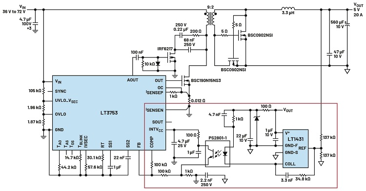
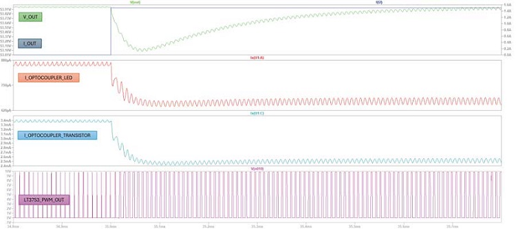
Based on the Figure 1 circuit diagram connection of the shunt regulator and optocoupler, let’s look at the LTspice sample simulation of the LT3753/LT1431 demo circuit 80 W active-clamp nonsynchronous forward converter for power over Ethernet (PoE) during transient load.
As illustrated in Figure 2, the power supply exhibits a dynamic response when exposed to a transient load specifically when the output current experiences a sudden step change from 0 A to 1.5 A. This abrupt increase in load demand introduces a temporary disturbance in the system’s steady state, as a voltage sag at the output. The sag occurs because the system was initially operating under no-load conditions, where only minimal energy transfer was required to maintain the output voltage. Consequently, the energy stored in the magnetic components and output capacitors is insufficient to immediately support the increased current demand.
This transient condition disrupts the steady-state operation, triggering the system’s feedback control mechanism. The feedback circuitry continuously monitors the output voltage and promptly detects the deviation from its nominal value. Upon identifying the voltage drop, it generates a corrective signal that is transmitted to the primary-side PWM controller.
In response to this signal, the PWM controller dynamically adjusts the duty cycle of the switching waveform. Specifically, it increases the on-time of the primary switching transistor, thereby extending the conduction period. This adjustment allows for a greater amount of energy to be magnetically coupled through the transformer during each switching cycle. The increased energy transfer compensates for the higher load current, enabling the output voltage to recover toward its regulated value.
As the system transitions to the new load condition, the output voltage stabilizes, demonstrating effective closed-loop regulation. The waveform analysis underscores the critical role of optocoupler biasing in maintaining loop integrity. For optimal performance, the LED within the optocoupler must be driven with sufficient forward current to ensure a linear optical response, while the phototransistor must be biased within its active region to accurately modulate the feedback signal.
Improper biasing—such as selecting an incorrect series resistor on the LED side—can significantly alter the CTR, which is a key parameter defining the efficiency of signal coupling between the LED and phototransistor. A reduced CTR can weaken the feedback signal, causing the PWM controller to underreact to voltage deviations, while an excessively high CTR may lead to overcompensation and instability. These effects are particularly pronounced during transient events, where the system must respond quickly to sudden changes in load. Inadequate biasing can result in delayed correction, voltage overshoot or undershoot, and degraded loop bandwidth.
The observed waveforms underscore the importance of precise component selection and biasing in the feedback path. Parameters such as LED forward voltage, CTR tolerance, phototransistor collector current, and compensation network design must be carefully considered to ensure robust transient response, stable voltage regulation, and reliable system performance across a wide range of operating conditions. Proper optocoupler biasing not only enhances loop accuracy but also contributes to improved electromagnetic interference (EMI) immunity and long-term reliability in isolated power supply applications.
iCoupler vs. Optocoupler: A Paradigm Shift in Isolation
Modern switch-mode power supply (SMPS) designs are increasingly adopting iCoupler digital isolation technology as a superior alternative to traditional optocouplers, particularly in applications demanding high speed communication, robust reliability, and long-term performance. Traditional optocouplers function by converting electrical signals into light using an LED, which is then detected by a phototransistor on the receiving side. While this method has been widely used for decades, it suffers from several inherent limitations, most notably LED aging, which leads to degradation in signal integrity over time, thus reducing reliability.
In contrast, iCoupler technology, pioneered by ADI, employs chip-scale microtransformers fabricated using standard CMOS processes to transmit digital signals across an isolation barrier. This transformer-based approach eliminates the need for light emission and detection, resulting in superior temperature stability, lower power consumption, and longer operational life. Unlike optocouplers, iCoupler devices are not susceptible to temperature-induced drift or LED wear-out, making them ideal for harsh environments and mission-critical systems.
From a performance standpoint, iCoupler devices support higher data rates—often exceeding 100 Mbps. This makes them particularly well-suited for digital control loops, telemetry, and high speed communication interfaces in SMPS architectures. Additionally, iCoupler solutions often integrate multiple isolation channels, DC-to-DC converters, and diagnostic features into a single package, reducing board space and simplifying design complexity.
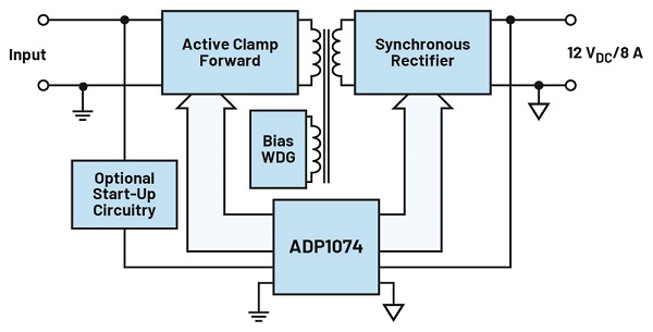
While optocouplers remain prevalent in analog feedback loops due to their simplicity and cost-effectiveness, they are increasingly being replaced in digital domains where precision, speed, and reliability are paramount. For example, in Figure 3, the ADP1074 integrates iCoupler isolation with a synchronous PWM controller, meets safety and regulatory standards, with advanced fault protection, offering a compact and highly integrated solution for isolated DC-to-DC converters in industrial, automotive, and telecom applications.
The shift toward iCoupler technology in modern SMPS design reflects a broader industry trend toward higher integration, greater efficiency, and enhanced reliability, enabling power systems to meet the stringent demands of next-generation electronic systems.
Conclusion
The LT3753-based isolated forward converter demonstrates effective transient load regulation through its feedback loop, driven by the LT1431 shunt regulator and optocoupler. Simulation results highlight the importance of precise optocoupler biasing and CTR in ensuring fast and accurate duty cycle modulation. Improper biasing can distort feedback signals, leading to delayed or unstable voltage correction—especially during load transients. In contrast, isolation technologies like iCoupler offer improved bandwidth and reliability, making them ideal for high speed or digital feedback systems. Ultimately, designing a robust feedback loop requires careful attention to component behavior under real-world conditions such as temperature drift and aging. Whether using the LT3753 or alternative controllers, the principles discussed here provide a solid foundation for achieving stable, responsive, and high performance power supply regulation.
In summary, don’t let your feedback loop fall flat—bias your optocoupler right, and embrace innovative design strategies.


