


Wafer Exchange for Ferroelectric Memory Materials:
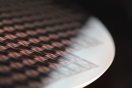
CEA-Leti and Fraunhofer IPMS have successfully completed the first exchange of ferroelectric memory wafers within the FAMES Pilot Line, marking a pivotal milestone in establishing a shared European platform for advanced embedded non-volatile memory (NVM) technologies. Launched in December 2023 and coordinated by CEA-Leti, the five-year initiative has demonstrated the viability of circulating complex material stacks across some of its leading research fabs.
The collaboration initially focused on the processing and electrical characterization of hafnium-zirconium oxide (HZO) ferroelectric capacitor stacks. Utilizing the combined 300 mm CMOS cleanroom capabilities of both institutes, they circulated the wafers in short process loops to enable joint evaluation of materials, electrode configurations, and device behavior.
The work also validated the wafer exchange and contamination-control protocols implemented in the pilot line, demonstrating that complex material stacks can be processed reliably across multiple advanced semiconductor facilities across all wafers.
The entire process adhered to standardized contamination control procedures, verified through VPD-ICP-MS (Vapor Phase Decomposition – Inductively Coupled Plasma Mass Spectrometry) and TXRF (Total Reflection X-Ray Fluorescence) analytics. Devices were evaluated using a ferroelectric capacitor (FeCAP) array test vehicle designed by CEA-Leti, with electrical characterization performed via the PUND (Positive-Up-Negative-Down) methodology to isolate true ferroelectric switching from parasitic effects.
‘Critical Insights’
“The successful wafer exchange marks an important step toward a joint European material-testing platform for ferroelectric memories,” said Dr. Wenke Weinreich, Division Director of Fraunhofer IPMS‘ Center Nanoelectronic Technologies, a member of the 11-member FAMES consortium. “By combining our processing expertise with CEA-Leti’s CMOS integration capabilities, the pilot line provides a powerful environment for evaluating new ferroelectric stacks and accelerating their path toward system-level applications.”
Initial experimental results have already yielded critical insights. The team screened various electrode materials to enhance performance, finding that titanium nitride (TiN) bottom electrodes significantly outperform tungsten. In reliability tests, TiN exhibited lower failure rates after 10⁷ field cycles at 4 MV/cm. Furthermore, clear cross-split effects were observed across different electrode configurations, confirming the sensitivity of the test vehicles to process variations.
Seamless Wafer Exchanges Across FAMES Sites
“This first exchange between CEA-Leti and Fraunhofer IPMS demonstrates that shared process flows, test vehicles, and characterization environments can work seamlessly across FAMES sites,” noted Dominique Noguet, pilot line coordinator and CEA-Leti vice president. “Establishing reliable wafer loops between leading research fabs is essential for accelerating ferroelectric memory development.”
Looking ahead, the wafer loops lay the groundwork for broader collaborative development. Upcoming phases will integrate HfO₂-based ferroelectric stacks from Fraunhofer IPMS into CEA-Leti CMOS processes, followed by array-level evaluations on GlobalFoundries’ 22nm FDX Memory Advanced Demonstrator Multi-Project Wafer shuttle prepared by CEA-Leti. This builds on Fraunhofer IPMS’ recent completion of a first chip tape-out using the same 22nm FDX technology, which also initiated research on algorithm-based AI compute-in-memory accelerator architectures. The roadmap further includes studies on electrode process variations, long-term reliability, and back-end-of-line (BEOL) integration approaches, such as nanosecond laser annealing (NLA).
Together, these efforts advance the core mission of the FAMES Pilot Line: to provide a unified European platform for developing and validating emerging memory technologies—including OxRAM, MRAM, FeRAM, and FeFET. By enabling collaborative material development and standardized characterization, the initiative aims to strengthen Europe’s capacity to design and manufacture the low-power, next-generation chip architectures required for the future of computing.


 Validation Solution for AI Networks")
