


Lattice Semiconductor Corporation (NASDAQ: LSCC), the leading provider of customizable smart connectivity solutions, today announced the availability of its Embedded Vision Development Kit, the first-of-a-kind development kit optimized for mobile-influenced system designs that require flexible, low cost, and low power image processing architectures. By leveraging a mix of Lattice’s FPGA, ASSP and programmable ASSP (pASSP) products in a single, modular platform, this unique solution provides the right balance of flexibility and energy efficiency required for a variety of embedded vision applications in the industrial, automotive and consumer markets.
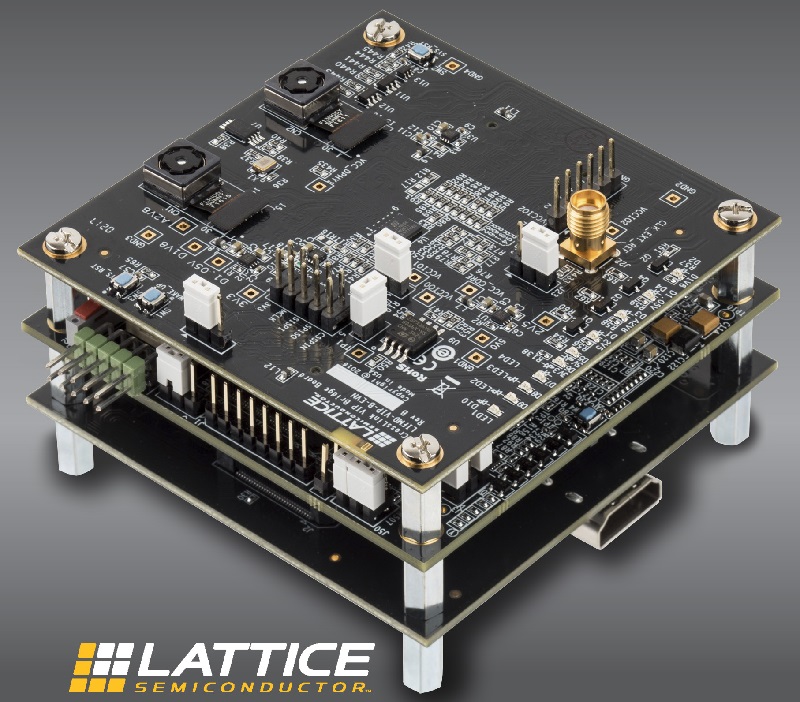
- Stackable boards based on Lattice’s CrossLink™ pASSP™, ECP5™ FPGA, and SiI1136 ASSP devices
- All-inclusive kit with stereo vision support, and dual MIPI® CSI-2 to 1080p HDMI® demo
- Optimized for low power, low cost, embedded vision applications in Industrial, Automotive, and Consumer markets
The new Embedded Vision Development Kit takes advantage of the company’s smart connectivity and acceleration product lines, equipping customers with a comprehensive, integrated solution for developing designs and enabling faster time-to-market. By combining the CrossLink pASSP mobile bridging device, ECP5 low power, small form factor FPGA, along with its high-bandwidth, high resolution HDMI ASSP, Lattice is offering an innovative solution that accelerates development of intelligent, vision-enabled devices at the edge.
 To enable and realize the true value of IoT, edge intelligence, which pushes processing for data intensive and processing applications away from the core to the edge of the network, continues to expand according to IDC. The market analyst firm has forecasted intelligent systems revenue to exceed $2.2 trillion in 2020.1
“As intelligence at the edge continues to increase, more applications will require integrated embedded vision technology,” said Deepak Boppana, director, product marketing at Lattice Semiconductor. “Our Embedded Vision Development Kit accelerates the adoption of mobile-influenced technology for applications including machine vision, smart surveillance cameras, robotics, AR/VR, drones and Advanced Driver Assistance Systems (ADAS).”
The CrossLink input board includes dual-camera HD image sensors supporting the MIPI CSI-2 interface, eliminating the need for external video sources. The ECP5 base board enables low-power pre/post processing and includes support for HD image signal processing (ISP) intellectual property (IP) from Helion Vision. Also included is a NanoVesta connector to support external image sensor video inputs. The HDMI output board based on the Sil1136 non-HDCP version enables connectivity to standard HDMI displays.
The Embedded Vision Development Kit is available now from Lattice and its distributors.
To learn more, visit www.latticesemi.com/evdkit.


