Imagine a future in which solar cells are all around us — on windows and walls, cell phones, laptops, and more. A new flexible, transparent solar cell developed at MIT is bringing that future one step closer.
The device combines low-cost organic (carbon-containing) materials with electrodes of graphene, a flexible, transparent material made from inexpensive and abundant carbon sources. This advance in solar technology was enabled by a novel method of depositing a one-atom-thick layer of graphene onto the solar cell — without damaging nearby sensitive organic materials. Until now, developers of transparent solar cells have typically relied on expensive, brittle electrodes that tend to crack when the device is flexed. The ability to use graphene instead is making possible truly flexible, low-cost, transparent solar cells that can turn virtually any surface into a source of electric power.

Photo: Stuart Darsch
Photovoltaic solar cells made of organic compounds would offer a variety of advantages over today’s inorganic silicon solar cells. They would be cheaper and easier to manufacture. They would be lightweight and flexible rather than heavy, rigid, and fragile, and so would be easier to transport, including to remote regions with no central power grid. And they could be transparent. Many organic materials absorb the ultraviolet and infrared components of sunlight but transmit the visible part that our eyes can detect. Organic solar cells could therefore be mounted on surfaces all around us and harvest energy without our noticing them.
Researchers have made significant advances over the past decade toward developing transparent organic solar cells. But they’ve encountered one persistent stumbling block: finding suitable materials for the electrodes that carry current out of the cell.
“It’s rare to find materials in nature that are both electrically conductive and optically transparent,” says Professor Jing Kong of the Department of Electrical Engineering and Computer Science (EECS).
The most widely used current option is indium tin oxide (ITO). ITO is conductive and transparent, but it’s also stiff and brittle, so when the organic solar cell bends, the ITO electrode tends to crack and lift off. In addition, indium is expensive and relatively rare.
A promising alternative to ITO is graphene, a form of carbon that occurs in one-atom-thick sheets and has remarkable characteristics. It’s highly conductive, flexible, robust, and transparent; and it’s made from inexpensive and ubiquitous carbon. In addition, a graphene electrode can be just 1 nanometer thick — a fraction as thick as an ITO electrode and a far better match for the thin organic solar cell itself.
Graphene challenges
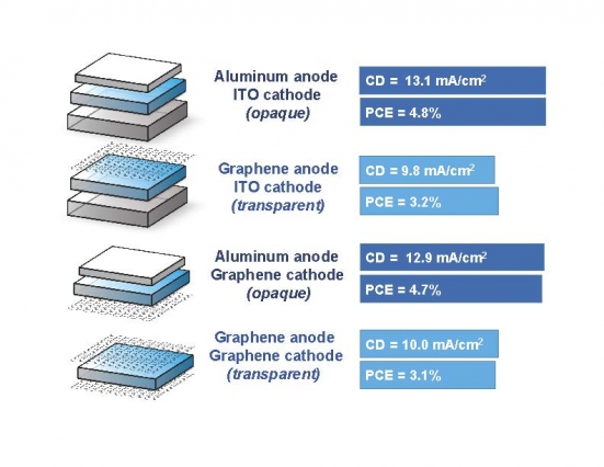
Two key problems have slowed the wholesale adoption of graphene electrodes. The first problem is depositing the graphene electrodes onto the solar cell. Most solar cells are built on substrates such as glass or plastic. The bottom graphene electrode is deposited directly on that substrate — a task that can be achieved by processes involving water, solvents, and heat. The other layers are then added, ending with the top graphene electrode. But putting that top electrode onto the surface of the so-called hole transport layer (HTL) is tricky.

Image courtesy of the researchers.
“The HTL dissolves in water, and the organic materials just below it are sensitive to pretty much anything, including water, solvents, and heat,” says EECS graduate student Yi Song, a 2016-2017 Eni-MIT Energy Fellow and a member of Kong’s Nanomaterials and Electronics Group. As a result, researchers have typically persisted in using an ITO electrode on the top.
The second problem with using graphene is that the two electrodes need to play different roles. The ease with which a given material lets go of electrons is a set property called its work function. But in the solar cell, just one of the electrodes should let electrons flow out easily. As a result, having both electrodes made out of graphene would require changing the work function of one of them so the electrons would know which way to go — and changing the work function of any material is not straightforward.
A smooth graphene transfer
For the past three years, Kong and Song have been working to solve these problems. They first developed and optimized a process for laying down the bottom electrode on their substrate.
In that process, they grow a sheet of graphene on copper foil. They then transfer it onto the substrate using a technique demonstrated by Kong and her colleagues in 2008. They deposit a layer of polymer on top of the graphene sheet to support it and then use an acidic solution to etch the copper foil off the back, ending up with a graphene-polymer stack that they transfer to water for rinsing. They then simply scoop up the floating graphene-polymer stack with the substrate and remove the polymer layer using heat or an acetone rinse. The result: a graphene electrode resting on the substrate.
But scooping the top electrode out of water isn’t feasible. So they instead turn the floating graphene-polymer stack into a kind of stamp, by pressing a half-millimeter-thick frame of silicon rubber onto it. Grasping the frame with tweezers, they lift the stack out, dry it off, and set it down on top of the HTL. Then, with minimal warming, they can peel off the silicon rubber stamp and the polymer support layer, leaving the graphene deposited on the HTL.
Initially, the electrodes that Song and Kong fabricated using this process didn’t perform well. Tests showed that the graphene layer didn’t adhere tightly to the HTL, so current couldn’t flow out efficiently. The obvious solutions to this problem wouldn’t work. Heating the structure enough to make the graphene adhere would damage the sensitive organics. And putting some kind of glue on the bottom of the graphene before laying it down on the HTL would stick the two layers together, but would end up as an added layer between them, decreasing rather than increasing the interfacial contact.
Song decided that adding glue to the stamp might be the way to go — but not as a layer under the graphene.
“We thought, what happens if we spray this very soft, sticky polymer on top of the graphene?” he says. “It would not be in direct contact with the hole transport layer, but because graphene is so thin, perhaps its adhesive properties might remain intact through the graphene.”
To test the idea, the researchers incorporated a layer of ethylene-vinyl acetate, or EVA, into their stamp, right on top of the graphene. The EVA layer is very flexible and thin — sort of like food wrap — and can easily rip apart. But they found that the polymer layer that comes next holds it together, and the arrangement worked just as Song had hoped: The EVA film adheres tightly to the HTL, conforming to any microscopic rough features on the surface and forcing the fine layer of graphene beneath it to do the same.
The process not only improved performance but also brought an unexpected side benefit. The researchers thought their next task would be to find a way to change the work function of the top graphene electrode so it would differ from that of the bottom one, ensuring smooth electron flow. But that step wasn’t necessary. Their technique for laying down the graphene on the HTL actually changes the work function of the electrode to exactly what they need it to be.
“We got lucky,” says Song. “Our top and bottom electrodes just happen to have the correct work functions as a result of the processes we use to make them.”


