


Any Printed Circuit Board (PCB) has its unique functionality and design. Apart from the various interconnects made of metals like copper and aluminium, the highly dielectric fiberglass is used for the base. The assembled PCB is a board with all the components required stuck on the same. The process of constructing a PCB board with its components is called PCB assembly. The metallic traces present- the lines seen running along with the board help in connecting the various parts of the PCB together. Presence of traces instead of wires helps in reducing the space, and in turn the resistance of the circuit. The essence of the PCB is achieved through the PCBA process.
THE ASSEMBLY PROCESS
The process begins with material preparation. The base of the PCB is dielectric composite materials. On top of the base, the copper layers are added, to provide electrical connectivity for the signals to pass through them. A solder mask is applied on top of the PCB to prevent short circuits from occurring. Short circuits are prevalent as the traces are minute with minimal widths to reduce resistance and hence increase the speed of the circuit. Holes are drilled in the solder mask to allow placement of the onboard components and make the PCB fully functional. On top of the solder mask lies the silkscreen. This provides labels for all the components on the board.
The first step in the process is solder paste stenciling. Here a mechanical fixture holds the PCB board in place. The stencil is held on top of the board, and the solder paste is only applied to those places where the components need to be placed. It like stenciling letters on a drawing paper, where kids can easily fill them with colors of their choice. An applier lays out the solder paste evenly. Once the stencil is removed the solder paste is present only in the required locations as given by the function sheet to the manufacturer.
The next step is called pick and place. It is similar to gluing images within predefined boxes for a pictorial chart. Earlier the process was manual. Tweezers were used to carefully place the intended components in their respective places for their usage. However, now the entire process has become automated increasing the accuracy and efficiency of the process. A robotic arm first picks the soldered board and places it at the station for placement.
Once the solder paste is allowed to dry(reflow soldering) with the use of heating ovens, which heat them to high temperatures followed by coolers that reduce their temperatures, help in controlled cooling of the solder paste and hence perfect stabilization of the onboard components. Reflow process can sometimes result in poor connection quality and shorts.
The process of inspection and quality control helps in overcoming the mistakes of reflow soldering. There are a number of ways to determine the worth of a PCB. Manual inspection is a good choice for a small batch of PCBs. But as the batch size increases, close inspection leads to optical fatigue and can increase the chances of errors. Automatic optical inspection uses multiple cameras to view PCBS in different angles. Quality of PCB is determined by the light it reflects. The AOI can detect the lower quality PCB at an alarmingly fast pace with high accuracy. X-rays can be used to view multiple layers and determine the quality of the PCB. Multiple checks are desirable as the errors can be diagnosed and rectified in the early stage of manufacturing itself. Following the inspection, the plated through-hole components are put in place manually or automatically. After the through hole process inspection, the above steps can be run in tandem for checking errors.
The final inspection is known as the functional test. The PCB, as the name suggests is tested for its functionality. The board is driven by the signals- for corners. The corners are the adverse condition any signal can pertain to. All the signals are continually monitored for any fluctuations or unacceptable behavior. If any unnerving characteristic is visible, the PCB fails its test and is scraped.
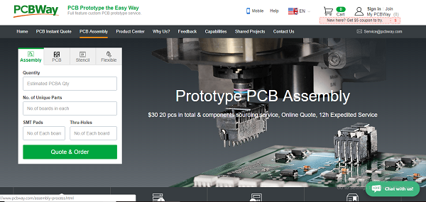
PCBWAY, the leading player in the PCB industry, along with PCB fabrication provides PCB Prototype assembly under its PCBA services domain. It offers PCB assembly services for low-mid volume production and Prototype quantities. PCBWAY team comprised of professional engineers and technicians who work closely with you for getting your PCB in best quality and quickest possible lead time.
PCBWAY assembly service provides assembling BGA, Micro-BGA, QFN and other leadless package parts. The PCBWAY assembly service offer SMT Assembly, BGA Assembly, Through-Hole Assembly, Mixed Assembly, Rigid Flex PCB Assembly Services. They check Inspection and Functional testing very closely. PCBWAY is the one destination for all your PCB needs, right from ordering all the components, PCB manufacturing, PCB assembly, testing and final shipment. They also provide various offers time-to-time. Currently, PCBWAY is offering a flash sale for its PCBA services, under which SMT fees dropped down from $88 to $30 for 1-20 pcs.
TECHNOLOGIES
Widely, two types of technologies are used in manufacture.
Surface Mount Technology: Small, sensitive components are mounted directly on the surface of the PCB board.
Through-Hole Technology: This process is used for larger components like capacitors and coils. Here, the lead of components are drilled through the base of the PCB and soldered on the other side.
The entire process of PCBA is a combination of mechanical and electrical devices working in harmony. The process is called an electro-mechanical assembly.
Challenges: Electrostatic Discharge (ESD)
Since PCBs contain thin traces of copper, running close to each other, carrying charges, this can cause Electrostatic Discharge- the phenomenon that causes lightning. It is the process of a sudden spike in voltage when two current-carrying components are in close quarters to each other. This generates an electromagnetic field which is not acceptable. ESD in a PCB can be caused when an object carrying the opposite charge comes close- it can be a person or another circuit. The fault can be catastrophic- either the reliability of the PCB is lost as it is degraded or the ESD can render it useless.
ESD detection and protection should be taken care of from the assembly process itself. The manufacturer must offer careful inspection of the PCB before it is dispatched. Circuit loops have to be avoided. Line lengths and parasitic inductances have to be measured and sufficient ground plane utilization should be present. ESD in operations too should be minimized.
PCB Manufacturing Trends and their Impact
Due to the increase in EU Automation, customer demands and development of technology, a sea change has appeared in the PCB manufacturing process. There is a rise in demand to produce small, compact devices. As the world moves towards the concept of nanotechnology, people aspire to own smart miniature devices with good durability and portability. There is a rise in the production of lead-free compliances to abide by the ‘Go- green’ initiative. Advanced quality testing mechanisms have come in place to ensure the nature of the PCB and give it a thumbs up for use. It has become essential to avoid customer dissatisfaction and short-life. 3-D integration allows better system performance, increased complexity and reduced costs as the area of the board is minimized. The reduction in the size of the PCBs has helped pave the road to application in different domains- nanotechnology, medicine, cellular technology, and consumer electronics.
With the increase in demand and reliability, Printed Circuit Boards have unrealistic standards set on them by the market. However, with a parallel growth in the electromechanical assemblies, it has become possible to attain the goals and expectation set by the community and make PCB ubiquitous.


