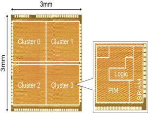
Renesas Electronics Corporation has developed an AI accelerator that performs CNN (convolutional neural network) processing at high speeds and low power to move towards the next generation of Renesas embedded AI (e-AI), which will accelerate increased intelligence of endpoint devices. A Renesas test chip featuring this accelerator has achieved the power efficiency of 8.8 TOPS/W , which is the industry’s highest class of power efficiency. The Renesas accelerator is based on the processing-in-memory (PIM) architecture, an increasingly popular approach for AI technology, in which multiply-and-accumulate operations are performed in the memory circuit as data is read out from that memory.
To create the new AI accelerator, Renesas developed the following three technologies. The first is a ternary-valued (-1, 0, 1) SRAM structure PIM technology that can perform large-scale CNN computations. The second is an SRAM circuit to be applied with comparators that can read out memory data at low power. The third is a technology that prevents calculation errors due to process variations in the manufacturing. Together, these technologies achieve both a reduction in the memory access time in deep learning processing and a reduction in the power required for the multiply-and-accumulate operations. Thus, the new accelerator achieves the industry’s highest class of power efficiency while maintaining an accuracy ratio more than 99 percent when evaluated in a handwritten character recognition test (MNIST).
Renesas presented these results on June 13, at the 2019 Symposia on VLSI Technology and Circuits in Kyoto, Japan, June 9-14, 2019. Renesas also demonstrated real-time image recognition using a prototype AI module in which this test chip, powered by a small battery, was connected with a microcontroller, a camera, other peripheral devices, and development tools at the demonstration session.
Until now, the PIM architecture was unable to achieve an adequate accuracy level for large-scale CNN computations with single-bit calculations since the binary (0,1) SRAM structure was only able to handle data with values 0 or 1. Furthermore, process variations in the manufacturing resulted in a reduction in the reliability of these calculations, and workarounds were required. Renesas has now developed technologies that resolve these issues and will be applying these, as a leading-edge technology that can implement revolutionary AI chips of the future, to the next generation of e-AI solutions for applications such as wearable equipment and robots that require both performance and power efficiency.
Key Features of the Newly Developed Technology for Next-Generation AI Chips:
Ternary (-1, 0, 1) SRAM structure PIM that can adjust its calculation bit number according to the accuracy required
The ternary (-1, 0, 1) SRAM structure PIM architecture adopts a combination of a ternary memory with a simple digital calculation block to hold increases in the amount of hardware and increases in calculation errors to a minimum. At the same time, it allows switching the number of bits between, for example, 1.5-bit (ternary) and 4-bit calculations according to the required accuracy. Since this can support different required accuracies and calculation scales on a per-user basis, users can optimize the balance between accuracy and power consumption.
High-precision/low-power memory data readout circuit that combines comparators and replica cells
When a PIM architecture is adopted, memory data is read out by detecting the value of the bit line current in the SRAM structure. Although it is effective to use A/D converters for high-precision bit line current detection, this approach has the issue of high-power consumption and increased chip areas. In this effort. Renesas combined a comparator (1-bit sense amplifier) with a replica cell in which the current can be controlled flexibly to develop a high-precision memory data readout circuit. Furthermore, these technologies take advantage of the fact that the number of nodes (neurons) activated by neural network operation is very small, about 1%, and achieves even lower power operation by stopping operation of the readout circuits for nodes (neurons) that are not activated.
Variation avoidance technology that suppresses calculation errors due to process variations in the manufacturing
The PIM architecture has the challenge of calculation errors due to process variations in the manufacturing. This is because process variations in the manufacturing cause errors in the values of the bit line currents in the SRAM structure, and as a result, errors occur in the memory data readout. To resolve this issue, Renesas covered the inside of the chip with multiple SRAM calculation circuit blocks and used blocks with minimal manufacturing process variations to perform the calculations. Since the activated nodes are only a small minority of all nodes, activated nodes are allocated selectively to SRAM calculation circuit blocks that have minimal manufacturing process variations to perform the calculations. This allows calculation errors to be reduced to a level where they can be essentially ignored.
Since introducing the embedded AI (e-AI) concept in 2015, Renesas has moved forward with the development of several e-AI solutions. Renesas has defined “classes” based on the effectiveness of e-AI and applications that are implemented and has been developing e-AI solutions based on the following four classes:
- Class 1: Judging the correctness or abnormality of signal waveform data.
- Class 2 (100 GOPS/W class): Judging correctness or abnormality using real-time image processing.
- Class 3 (1 TOPS/W class): Performing recognition in real time.
- Class 4 (10 TOPS/W class): Enabling incremental learning at an endpoint.
Renesas introduced an e-AI development environment in 2017, and in 2018 announced the RZ/A2M microprocessor, which integrates Renesas’ exclusive DRP (dynamically reconfigurable processor) on chip. Renesas provides these technologies for applications classified through class 2. To implement class 3 applications, Renesas has further improved the computational performance of this DRP technology.
Now, Renesas is unveiling the new, leading-edge technology developed through this effort. The new accelerator technology combines both low power consumption and improved computational performance and could be one of the key technologies to implement future class 4 applications. Renesas is committed to contributing to the realization of a smart society through increased intelligence that applies AI at both edges and endpoints in the IoT.


