


The Internet of Things (IoT) comprises billions of devices, and each of these nodes has the potential to be compromised, even before installation, if it incurs physical damage while being shipped from the manufacturer to the installation location. The environment it is deployed in can also have an impact, especially if it is hot or humid or there is a significant amount of vibration present. Depending on where devices are deployed, there is always the potential for people to physically interfere with them, or execute a security breach by some other method. However, mesh networks are eliminating the “weakest link in the chain” issue as the multiplicity of nodes and various paths provide a high degree of redundancy – unless one of the end nodes fails.
MarketsandMarkets has estimated that there will be over 17 billion operational IoT nodes by 2023, although other estimates put this number even higher. Whichever number is correct, the task of ensuring security for each and every node and overall network integrity is a massive challenge. Part of the solution is for these nodes to become more intelligent, gaining the ability to check for internal malfunctions and perform other important self-checks as well as ensuring integrity for any data received or transmitted. If an IoT node included a basic accelerometer then, should a drop occur during transport, the severity of the fall could be captured and the microcontroller alerted. Other sensors could determine the orientation of the node as it hit the floor, and the microcontroller could process this data to determine the likelihood that the node had been damaged.
The node could then send a message via an IoT gateway to let the manufacturer, shipping company or customer (or all three) know about the damage and the need for replacement. In order to deliver this functionality, designers need to consider all aspects of the system, especially the MCU, sensors, power management, wireless connectivity and memory. Central to this is the MCU, which must support the ability to self-diagnose so that this functionality can be implemented.
Depending on the sophistication of the node, how much power is available and the amount of data requiring processing, most IoT nodes will use either a 16-bit or 32-bit MCU. If the node is at the end of the mesh or is used as a gateway, it will almost certainly use a 32-bit MCU to process the more sophisticated algorithms that are necessary. Many will include encryption – AES-256 is quite common.
16-bit MCUs that are Power Efficient
The PIC24E family of 16-bit MCUs from Microchip comprises general-purpose 16-bit MCUs that offer high performance, enhanced code density and can deliver 70MIPS throughput from a single 3.3V supply. The fully featured devices include op-amps, motor control, enhanced ADCs, DMA channels for fast data throughput and USB OTGs, and have CAN bus communication capability. Suitable for rugged applications, they can operate in temperatures up to 150°C and offer memory options to 536kB, while occupying footprints as small as 5mm x 5mm.
Texas Instruments offers over 25 different package configurations with varied peripheral configurations in its MSP430 series of ultra-low-power MCUs. Devices in the series incorporate powerful 16-bit RISC CPUs, Flash memory (up to 512kB) and RAM (up to 64kB). There are also a number of methods to maximize code efficiency, including 16-bit registers. They can be woken into active mode in under 6µs, due to oscillators that incorporate digital control.
The high levels of integration available in the MSP430 series mean that both analog and digital peripherals are included to reduce system BoM costs and enhance performance, while simplifying the design process. Peripherals available include op-amps, comparators, timers and data converters, as well as more sophisticated devices such as ultrasonic sensing and capacitive touch. A variety of low-power modes allow the MCUs to balance power consumption and performance, achieving <100μA/MHz while retaining the contents of the RAM, which consumes just 0.1μA. A <1μA RTC mode enables a typical IoT battery to last as long as 20 years.
32-bit MCUs for IoT Applications
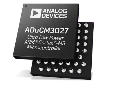
Based on 32-bit ARM Cortex-M3 processor cores, Analog Devices’ ADuCM3027 and ADuCM3029 ultra-low-power MCUs are simple to configure to achieve balance between performance and power consumption – while maintaining the security and reliability demanded by IoT applications. The devices are suited to a variety of IoT-centric applications including building/factory automation, smart energy, healthcare and smart agriculture.
Both models include ECC encryption; in fact, the only difference is the available Flash memory – 128kB or 256kB. Using the Embedded Microprocessor Benchmark Consortium (EEMBC) evaluation technique, these MCUs achieve a 245.5 ULPBench score. When running in full-on mode the devices typically require <30μA/MHz, while in flexi mode, where the core is powered down but the peripherals remain active, this reduces to a typical value of <300μA. For the highest level of power saving the devices can be put into hibernate mode, where the contents of SRAM are retained – this typically consumes <750nA.
Strong read protection is delivered by several hardware and software protection mechanisms that effectively prevent any unauthorized reading of device content. Write protection prevents unauthorized reprogramming, preventing malicious code being injected. Error correction on the Flash memory and voltage monitoring when in standby mode prevent corruption of code or data that could result in system crashes that leave them vulnerable.
The Synergy S3A1 MCUs from Renesas contain a 48MHz 32-bit ARM Cortex-M4 CPU core along with a floating point unit (FPU) and several analog devices. The MCUs include multiple security features and have 1MB of Flash memory for the storage of code as well as a further 8kB of Flash for data and 192kB of SRAM. As part of the wider Synergy MCU product range, the S3A1 devices are fully compatible (pinout, features, IP) with other devices in the range, allowing code reuse and scalability to speed up the design process. These devices are suited to a wide variety of applications, but are particularly popular in monitoring applications where regular firmware updates are necessary to maintain and upgrade features.
A 180MHz ARM Cortex-M4 core drives NXP Semiconductors’ LPC540 32-bit MCUs, which also include advanced HMI capabilities, an efficient power architecture and flexible communications. Further flexibility is delivered by a quad SPI, graphic LCD, 11 FlexComm channels and CAN bus capability – enabling the devices to be reconfigured as applications evolve. Commonality throughout the product series allows for easy migration to enhanced processing power or additional peripherals when necessary. LPC540 devices include 360kB of RAM, a TFT LCD controller and a pair of CAN FD modules as well as Ethernet connectivity. They are supplied in a variety of packages including TFBGA180, TFBGA100, LQFP208 and LQFP100. Requiring just 100µA/MHz when operating in active mode, the advanced MCUs strike a good balance between integration of functionality and efficient use of available power.
Also based on an ARM Cortex-M4 32-bit RISC core, this time operating at frequencies up to 80MHz, are devices in STMicroelectronics’ STM32L4 family of ultra-low-power MCUs. These devices incorporate a precision-format FPU that supports every ARM single-precision data-processing instruction and data type as well as a full set of DSP instructions. The devices enhance the security of applications via an included memory protection unit.
The family offers ultra-low power consumption as a result of the FlexPowerControl technology that is included, allowing the achievement of a EEMBC ULPBench score of 150 ULPBench-CP. The 80MHz ART accelerator enables the system to achieve 100DMIPS/273 CoreMark, while DMA controllers and a multi-AHB bus matrix optimize system performance. Memory resources include 2MB of dual-bank Flash and 640kB of SRAM. As the STM32L4 is fully pin-compatible with the earlier STMF32, designs can be easily upgraded to take advantage of lower power consumption, without needing time-consuming and risky PCB changes.
Small-Size MCUs
Cypress Semiconductor’s PSoC 6 MCU is an all-in-one solution that provides the necessary security and processing performance for IoT applications. The dual-core device is based on ultra-low-power 40nm process technology and uses an ARM Cortex‑M0+ for tasks where power consumption is critical, utilizing the ARM Cortex‑M4 where performance is the primary consideration. When active, the M4 core consumes 22μA/MHz while the M0+ core is more frugal at just 15μA/MHz.
The flexible architecture allows peripheral features including Bluetooth Low Energy (BLE) and USB to be added, as well as enabling the development of custom analog front ends and digital interfaces for IoT applications. Security is assured through the inclusion of various encryption protocols, including ECC and AES – as well as secure hash algorithms.
The SAM R34 from Microchip is a LoRa sub-GHz system-in-package (SIP) family that is intended to reduce design times by including a LoRa transceiver and software stack along with a high-performance 32-bit MCU with ultra-low power consumption. Interoperability with LoRaWAN gateways and network providers has been proven, and certified reference designs are available.
Designers looking for a highly flexible single-chip solution intended for short-range wireless applications should consider Nordic Semiconductor’s nRF52840 multi-protocol SoC. The embedded 2.4GHz transceiver supports a variety of protocols including Bluetooth 5/BLE, 802.15.4/Thread and ANT/ANT+, and also some proprietary 2.4GHz protocols. The multi-protocol feature is dynamic, enabling simultaneous Bluetooth 5 and Thread connectivity, and carefully sharing time to ensure that both protocols maintain connectivity.
The nRF52840 features a 32-bit, 64MHz ARM Cortex-M4F CPU with 1MB Flash memory and 256kB of RAM with a configuration that enables DSP instructions, hardware acceleration of FPU calculations, single-cycle multiply and accumulate, and hardware divide for low-power execution of complex calculations. The MCUs can operate from primary or secondary batteries, as well as directly from USB due to the wide input range of 1.7V to 5.5V. Battery life is maximized through management of power usage and resources, including the ability to switch supplies, and turning off unused peripherals to save power.
Developing IoT solutions can be a challenging task, balancing the need for small size, ultra-low power consumption, performance and comprehensive function sets – and a wide range of peripheral availability. Fortunately, advanced technology is becoming available which will help designers meet these challenging objectives in this rapidly growing area of technology.


