Every day, millions of packages, many containing valuable or perishable goods, are shipped by courier delivery companies to locations all around the world. It’s estimated that UPS alone moves almost 16m packages every day. It’s a huge undertaking to make sure every package gets to its final destination reliably, on time and most importantly, undamaged.
For many of these shipments, the products they contain are sensitive to environmental conditions such as temperature and shock, which can often be a problem if not managed carefully during shipment. Products such as fresh flowers, fruit and vegetables, and medicines are all shipped in vast numbers every day, but each shipment needs to be handled with care, making sure they do not suffer from physical damage and are kept within the optimum storage and shipment conditions. If they are not maintained in such a way during shipment, they may not arrive at the final point of delivery in a suitable state to be used by the end customer. In the case of some items such as medicines, they can be rendered dangerous or, at the very least, ineffectual. Vaccines are a perfect example of such an item, as they must be handled in the correct manner and kept within the correct environmental conditions at all times to avoid potentially serious medical consequences.
A new generation of smart products, capable of tracking these parcels and constantly monitoring how they are handled and the local environmental conditions during shipment has grown up around the need to provide a detailed audit trail of the shipment.
Today, these tracking products are typically battery operated and are able to measure parameters such as temperature and acceleration. Some can even track GPS location during shipment and store the information for future examination once the product has been delivered. It’s also important to ensure that they are not tampered with in any way or replaced by lower cost replicas, especially in the case of more valuable shipments.
However, these trackers are not without problems, especially around the use of battery technology. It’s becoming increasingly difficult to ship products containing batteries, especially by airfreight, due to the possibility of the batteries overheating. Using batteries also means that the battery must be charged before each shipment to make sure the device is able to operate for the whole duration of the shipment process – from initial shipment through to final delivery. The onus is on the initiator of the shipment to make sure the device is charged, a process which is always open to human error.
In these cases, a device that can supply energy from the environment during the shipment process, potentially avoiding the need for the device to contain a battery, could provide an ideal solution.

Let us look in more detail at how to resolve a typical issue – in this case, the problem of the reliable shipment of pharmaceutical products around the world. To get an idea of the scale of the problem, millions of euros worth of pharmaceuticals are prescribed by doctors across Europe every year. In Germany alone, medication worth over 40 billion euros was dispensed to patients in 2017, and the resultant shipment costs added billions of euros to the total annual bill. It’s currently estimated that the total costs of safe shipment of these products is in the US$70 – 80 billion range worldwide.
With such costs, we need to make sure that each product is delivered safely and efficiently to the end user, and has not suffered any degradation or been replaced by another product during the shipment process.
Intelligent solutions that use energy harvesting to power such shipment monitoring applications are now possible with a new generation of advanced, low-power embedded controllers. These are based on Renesas’ new Silicon on Thin Buried Oxide (SOTB) process technology. Devices based on the SOTB process exhibit significantly lower active and standby power consumption than devices using traditional bulk silicon technology. SOTB allows the development of extremely low- power, intelligent devices ideally suited for continuous monitoring of parameters such as temperature and acceleration during the shipment process. These devices can provide high processing performance for local processing and large on-chip memories for application and data storage. This allows the memory to contain complex applications and protocol stacks while providing non-volatile data storage for the logged information. This can all be achieved while operating from energy harvested from the environment, with no batteries required.

The first embedded controller to be implemented on this new process is the new R7F0E017. This device can achieve active power consumption of around 20 µA/MHz with operation at up to 32 MHz and leakage current down to 150 nA in deep standby mode. These figures are unmatched for a device with 1.5 Mbytes of on-chip flash and 256 Kbytes of SRAM on-chip.
Let us look in detail at this new technology and how it can help us to implement devices that are ideal for these PMA applications. The breakthrough in the development of this technology was the ability to create a hybrid silicon structure, combining the benefits of the new SOTB process and those of the existing standard bulk silicon technology. We can use the new SOTB technology in parts of the chip design where ultra-low power consumption is required. However, we can still use standard silicon for features such as the I/O ring and analogue components, as well as the embedded Flash memory. As a result, the devices still have similar electrical characteristics to today’s existing microcontrollers.
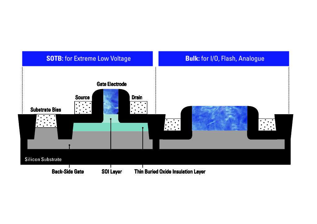
Figure 3 shows some of the benefits of the SOTB gate structure. In a traditional bulk silicon gate design, we inject dopant atoms into the silicon during the manufacturing process, which enables the gate to conduct when required. The number of atoms injected into each gate is extremely hard to control accurately, and so the gate switching characteristic can vary, especially with smaller silicon geometries.
SOTB is a dopantless design in which the gate characteristics are controlled by the extremely thin isolation layer within the gate, which itself is extremely well controlled. This means that the variation between each gate is much lower than with the traditional bulk silicon gate design. This reduction in the variation between gates on a SOTB device allows us to greatly reduce the operating voltage and hence the energy used to switch the gate. The result of this is the extremely low active power consumption of devices implemented on the SOTB process compared to devices implemented in a traditional bulk silicon process.
Figure 3 also illustrates another benefit of the SOTB technology. We can apply a negative back bias voltage to each gate, allowing us to manipulate the switching thresholds of each gate. This greatly reduces the leakage from each gate, which in turn reduces the standby current.
The new R7F0E017 combines a Cortex M0+ core running at up to 64 MHz with a high level of peripheral integration, up to 1.5 Mbytes of flash and 256 Kbytes of on-chip SRAM. Figure 5 shows a block diagram of this device. The R7F0E017 also implements an MiPs LCD interface for a low power local display as well as other useful functions, such as a USB interface and a very specific ultra-low power analogue to digital convertor (ADC). Every device also includes an energy harvesting controller (EHC) to help manage a variety of harvested power sources.
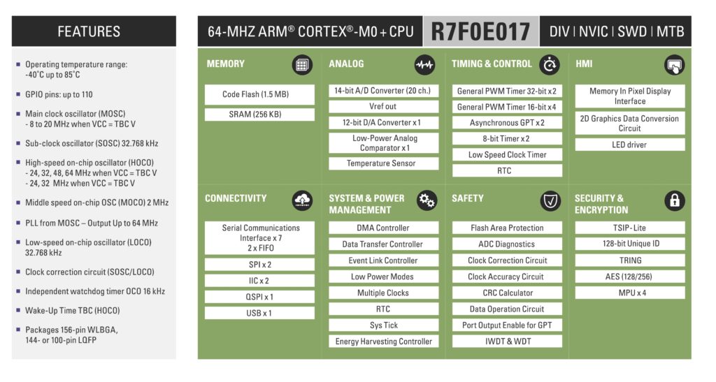
The ADC has a completely new design that has been specifically developed to operate from the minimum amount of energy, while still supporting the continuous sensing of various analogue parameters.
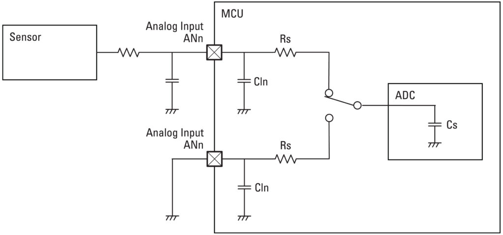
A simplified input diagram of the ADC is shown in Figure 5. The ADC was designed to support resolutions of up to 14 bits, giving the ability to make accurate measurements of many different physical parameters. The key benefit of this new ADC design is that it consumes only 3 µA when operating at 32 kHz, with a sample rate of 1.6k samples / second. This sample rate, while slow, is more than enough for the measurement of most parameters required in a tracking application, such as temperature and pressure as they normally change very slowly.
The ADC has also been designed to operate autonomously without CPU intervention, again minimising power consumption when used. These features include a variety of scan modes to automatically sample multiple channels, an automatic averaging circuit to increase the accuracy of the measurements, and a comparator function. The latter can generate an interrupt when the measured value is above, below or outside a pre-programmed range.
The ADC module also integrates an on-chip temperature sensor, which can be automatically monitored to check if the shipment temperature exceeds predetermined limits. The complete ADC subsystem is an ideal solution to many tracking applications, providing all the functions needed to monitor and log the environmental conditions affecting the shipment as well as minimising the power consumption required for this task.
The R7F0E017 also implements a unique energy harvesting controller (EHC) that allows energy to be harvested from a wide range of different renewable energy sources, while allowing the device to automatically control an external rechargeable battery or super capacitor. The EHC can also supply power to external devices such as radios and sensors so that they can also operate on harvested energy. This facilitates the development of a complete, batteryless solution for tracking applications that can be powered entirely by a variety of energy harvesting solutions, including harvesters that operate with vibration and light.
One of the biggest problems with any embedded device in energy harvesting applications is the “inrush” current. This is the current that the device requires when it is initially switched on and is typically quite large. The risk here is that it swamps most typical energy harvesting power sources and causes the device to operate incorrectly. The EHC implemented on the SOTB devices is designed specifically to avoid this issue. It has been developed to manage the small amounts of energy available from a harvesting power source to enable the safe and reliable start-up of the microcontroller from low energy power sources supplying as little as 5 µA of current. This means that, for almost the first time, real tracking applications are achievable and can use energy harvested from the environment to measure and log continuous data from their surroundings.
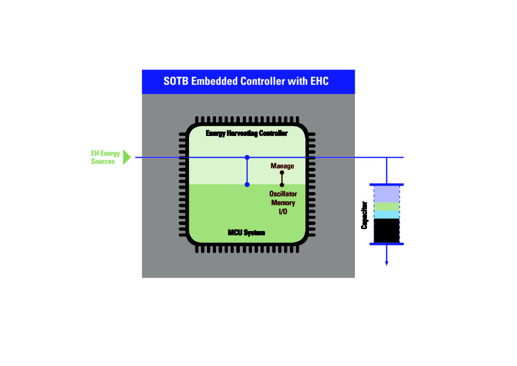
With the correct power dimensioning circuitry, the energy harvesting controller enables these devices to operate with a wide range of power sources including solar cells, vibration harvesters, thermal harvesters and many more. Many examples of these can be found on the Renesas website at www.renesas.com/SOTB along with videos showing some typical examples of harvesters in use.

The development of embedded controllers based on the Silicon on Thin Buried Oxide technology will enable a new generation of tracking applications designed to operate without a battery. In healthcare applications, these will improve product quality and condition while providing significant cost savings for the healthcare industry.
Samples of the R7F0E017 with the integrated energy harvesting controller, along with a complete suite of development tools, will be available to beta customers in early 2019 with general samples available in the second half of 2019.


