


Isolation is a means of preventing current flow between two communicating points while allowing data and power signal transmission between them. Isolation prevents high voltages from damaging sensitive electronic components or harming humans. It also eliminates ground loops in communication links with large ground potential differences to maintain signal integrity.
Over the past decade, legislation has changed and now requires machinery and equipment operating in harsh environments to implement isolation for their data transmission systems. As a result, the trend away from legacy single-channel isolated systems to applications utilizing multi-channel isolation has led to the introduction of new isolation components. Many of these applications involve data communication in telecommunication and industrial networks, medical systems, sensor interfaces, motor control and drive systems, and instrumentation.
This article focuses on isolated digital interfaces conforming to RS-485, which continues to be the industry’s workhorse standard for data transmission. Renesas’s will provide an overview of RS-485’s common-mode voltage range (CMVR) definition, and explain how isolating a transceiver’s signal and supply paths from the local controller circuit allow it to tolerate huge common-mode voltages. Finally, Renesas will present a new RS-485 isolator based on giant magnetoresistance (GMR) technology, and discuss its benefits over other isolation technologies.
Common-mode Voltage Range
The RS-485 standard specifies its common-mode voltage range from -7V to +12V. Figure 1 shows this range, including the driver output common-mode voltage (VOC), the ground potential difference between driver and receiver grounds (GPD), and the longitudinally coupled noise (VN).
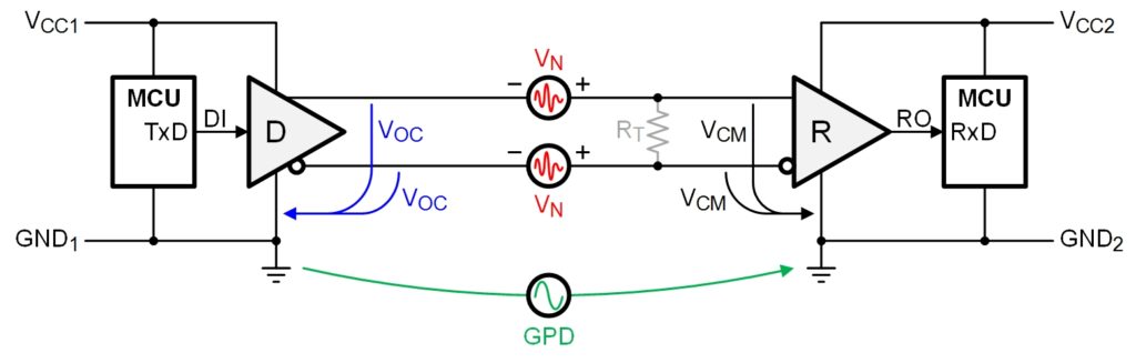
The driver is designed to generate a symmetrical, differential output (VD) around a common-mode component of VCM = VCC/2, thus making the line voltage at one output VA = VCC/2 ± VD/2, and the voltage at the complimentary output VB = VCC/2 ∓ VD/2.
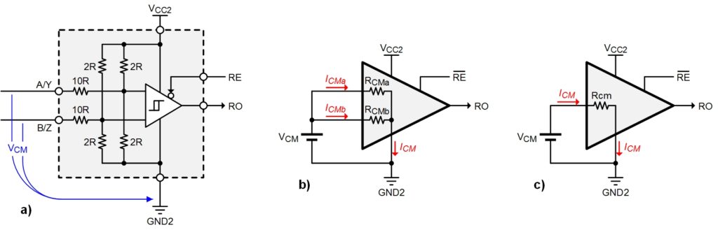
The receiver is designed to process only differential signals within the specified CMVR and to reject any common-mode components. This is accomplished by an internal voltage divider that equally attenuates both common-mode and differential signals (Figure 2). The subsequent differential comparator then builds the difference between the two attenuated input signals, thus amplifying only the differential component.
Since the voltage dividers represent common-mode resistances (RCM) between each receiver input and receiver ground, the entire common-mode voltage of the data link drops across these resistances. This means that for a standard transceiver, the receiver must correctly detect differential input voltages over the entire CMVR from -7V to +12V.
To tolerate higher common-mode voltages (VCM), such as ±25V, the transceiver bus I/O stages are redesigned such that the driver output transistors possess higher stand-off voltages and the receiver voltage dividers have higher divider ratios, which can also necessitate higher resistor values.
For very high common-mode voltages (in the hundreds of volts), the insertion of galvanic isolation barriers is required, which eliminate high voltages at the transceiver bus terminals.
Isolation Expands CMVR
Figure 3 depicts an example of an isolated data link in which only the receiver is isolated from its local controller. Proper galvanic isolation must include both power supply and data lines. With regard to the power-supply ports, an isolated DC/DC converter converts the Earth referenced supply rails of the microcontroller, VCC2 and GND2, into the isolated and floating supply rails, VCC2-ISO and GND2-ISO of the transceiver.
Isolation of the data path is provided through a digital signal isolator (ISO). Here the bus side of the isolator is supplied by VCC2-ISO and GND2-ISO, while the controller side of the isolator is supplied by VCC2 and GND2.
Because the current always returns to its source, there is no interaction between the isolated supply rails of the receiver and the non-isolated supply rails of the driver.
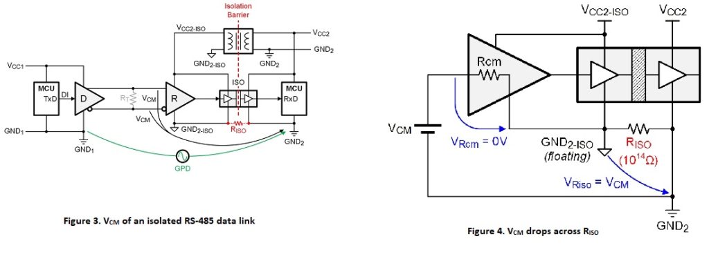
Figure 3 clearly shows that the ground potential difference (GPD) remains between the Earth referenced grounds of GND1 and GND2, as does and the common-mode voltage between the signal pair conductors and GND2. However, the isolation barrier has decoupled the receiver ground from GND2, thus converting it into the floating ground (GND2-ISO).
Figure 4 clarifies the situation by providing the common-mode equivalent circuit of the isolated receiver node. Because the huge resistance of the isolation barrier (RISO = 1014Ω) is in series with the receiver’s much lower common-mode resistance (RCM = 105Ω), the entire VCM drops across RISO, thus eliminating the common-mode impact across the receiver (VRcm = 0V). Additionally, the GND2-ISO potential tracks the receiver input voltage, so there is no worry about violating the receiver’s maximum input voltage relative to the receiver ground. Since VCC2-ISO also references GND2-ISO, the supply voltage across the isolated receiver maintains the proper value regardless of the common-mode voltage level.
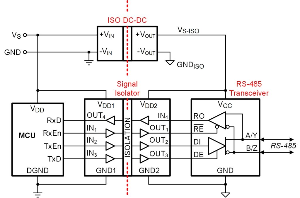
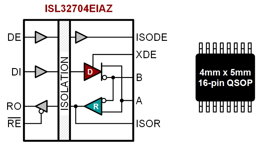
Note that Figures 3 and 4 show the isolation for only the receiver (Rx) data path, but an isolated RS-485 node requires four channels (see Figure 5) to handle the transmit and receive data paths, and the transmit and receive enable signals.
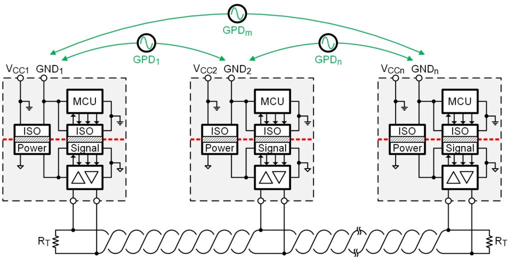
In a point-to-point connection, it is sufficient to isolate just one node to prevent a ground loop, leaving the other node non-isolated. But in multi-point data links, it is common practice to isolate every bus node in order to reuse circuit node design and to simplify PCB production. Figure 6 gives an example of an isolated multi-point bus.
Modern RS-485 isolation combines the isolator and the transceiver functions into a single chip, which contributes to tremendous space savings in bus node designs. The ISL32704E isolator in Figure 7 utilizes GMR technology, which further enhances small form factor designs by enabling the construction of the smallest, yet most robust isolation structures possible.
For example, optimized layout and design techniques made it possible to manufacture the 4mm x 5mm isolator QSOP package shown in Figure 7, while maintaining a whopping 600V of working voltage at a barrier lifetime of 44000 years. This is 50% more working voltage than the 400V working voltage of competing technologies providing 2.5kV functional isolation. Furthermore, the device is UL recognized and VDE certified.
The principle operation of a GMR isolator is highlighted in Figure 8. It shows a buffered input signal driving a primary coil, which creates a magnetic field that changes the resistance of the GMR resistors 1 to 4. GMR1 to GMR4 form a Wheatstone bridge to create a bridge output voltage that only reacts to magnetic field changes from the primary coil. However, the large external magnetic fields are treated as common-mode fields and are therefore suppressed by the bridge configuration. The bridge output is fed into a comparator whose output signal is identical in phase and shape to the input signal.
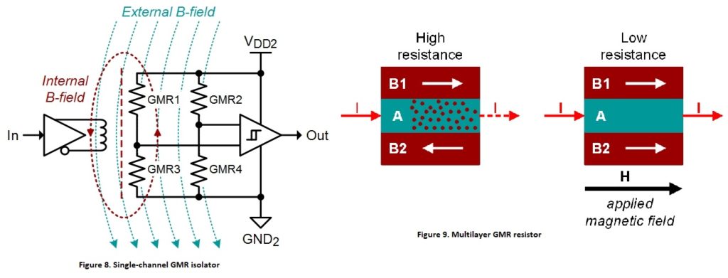
Figure 9 depicts the function of a single GMR resistor. This resistor consists of ferromagnetic alloy layers, B1 and B2, sandwiched around an ultra-thin, nonmagnetic conducting middle layer A, which is typically copper. The GMR structure is designed so that, in the absence of a magnetic field, the magnetic moments in B1 and B2 face opposite directions, thus causing heavy electron scattering across layer A, which drastically increases its resistance for current I. When a magnetic field H is applied, the magnetic moments in B1 and B2 are aligned and electron scattering is reduced. This lowers the resistance of layer A and increases current flow.
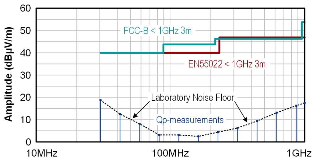
Unlike capacitive and magnetic isolators that necessitate RF carrier or pulse-width modulation (PWM) to transfer DC and low-frequency signals across the barrier, GMR isolators do not require such fancy encoding schemes. Nor do they include current hungry power transfer coils or transformers, as their signal transfer is virtually energy-less. The absence of the above factors not only results in a significantly lower current consumption (Figure 10), but also causes the radiated emission spectrum to be virtually undetectable (Figure 11). Furthermore, because GMR isolators have no pulse train of RF carriers to interfere with, they also have very low EMI susceptibility.
Conclusion

GMR is not just another isolation technology, but rather the isolation technology for high-speed and ultra-high-speed data transmission systems. Its virtual energy-less information transfer combined with a tiny form factor to ensure barrier propagation times in the sub-nanosecond range. The nanosecond prop-delays specified in the ISL32704E datasheet are mainly contributions of the I/O buffer and the transceiver.
GMR isolators do not replace optoisolators, mainly found in DC to 1Mbps applications, but provide complimentary isolation in the high and ultra-high frequency realms.The fact that GMR isolators are the only isolators immune to single-event and total ionizing dose radiation, makes this fine technology also applicable to space and military applications.


")


