


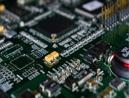
With the technology arising, it is needless to say that electronics have made our lives easier and people can hardly survive without them. All the electronics have a core component, PCB which is a self-contained unit integrated with the combination of multiple conductive copper foil layers. However, when the multilayer PCB is concerned, it is made out of combination of double-sided and single-sided PCB. Given the availability of multiple layers, the insulation and gluing together is explanatory. The layers are placed in a position to create the surface sides and connect to the surrounding environment.
The connections are attained through the hole plating, buried vias, and the blind vias as they are empowered to incorporate the required number of conducting layers for completing the project. The main reason for opting for multilayer PCBs is that electronic industry is undergoing dynamic shifts and the functionality is meant to be erudite. Back in the days, PCBs were cancelled out given the constraints regarding crosstalk, noise, and stray capacitance. However, getting rid of these constraints wasn’t possible with single and double-sided PCBs which gave rise to the multilayer PCBs. The size and thickness of the multilayer PCB varies according to the application; more or less ranges from four to twelve layers.
The number of layers is kept even as they are cost-effective, plus the odd numbers can lead to circuit warping. If we look at our handsets, they use almost twelve layers of PCB but in case of complex electronics, the number can reach up to one hundred. The main reason for using the multilayer PCB is that it increases the wiring area by incorporating minimum three conductive layers. In common scenarios, the layers are veneered on one board to keep it straightforward and streamlined rather than leading to wrapping and twisting. The layers are generally categorized as signal, ground, and power.
Construction
The multilayer PCBs are constructed by adjoining the pregpreg along with the core material. Once joined, high temperatures and pressures are endorsed to get rid of the air bubbles. The layers are sticked together using the adhesive material while resin is used to cover the corners and conductors. The most commonly used materials include epoxy glass, Teflon, and ceramic. The inculcation of pregpreg makes the PCB flexible and are endorsed in the lamination to get rid of air bubbles while joining them to perfection. Now, the PCB will be set aside to cool down and become the solid board to be used in the electronics.
Advantages
There are multiple advantages adhered to using the multilayer PCBs in the electronics and we have rounded up some of them in the section below;
- Compactness – This is the topmost advantage of using the multilayer PCB boards. The layers are adjoined together to save the space making it apt to be used in the advanced electronics. These are commonly used in laptops, smartphones, and tablets which define the importance of using multilayer PCB.
- High Power – The density is higher which enable the higher connectivity and innateness allows the users to capture the high speed and capacity within the compact size.
- Top-notch – Multilayer PCBs are more complex than single or double-sided PCBs and great deal of focus and effort goes into to. This embarks that the quality will be top-notch and will provide the reliable results.
- Durability – Multilayer PCBs come with reliable insulation while the layers are adjoined together through the pregpreg. The board is then laminated in the protective material which defines the durability.
- Lightweight – Given the compact design, the PCBs tend to be lightweight and is apt for the mobility in electronics.
- Flexibility – If the multilayer PCB has a fewer number of layers, the construction can be named flexible thus can be used in the electronics that need a little bending.
Downsides
Just like any other product, multilayer PCBs come with their own set of downsides as they aren’t appropriate for all types of electronics thus the application is limited.
- Costs – As compared to single and double-sided PCBs, the multilayer PCBs are higher in cost. The manufacturing is costly as well given the time that needs to be put in and the efforts regarding designing are high as well. However, given the error in manufacturing, the board will be faulty which will lead to double costs regarding material and labor.
- Production – The multilayer PCBs are very difficult to design, manufacture, and needs plethora of time and efforts to get the final product in hand.
But no matter what, the utilities of multilayer PCBs cannot be ignored at any point and it all falls down to the application or the electronics to be used in.


