


Technology delivers many advances that make our business and personal lives easier, safer and more enjoyable. However, as we become more reliant on technology in many, if not all, aspects of our daily lives, then the consequences and impact of failure, or worse still, a malicious attack, become more significant.
At the heart of many systems these days is an application specific integrated circuit (ASIC); a custom device that allows designers to create functionality optimised for the application. As ASICs are custom ICs they contain a significant amount of valuable intellectual property (IP). Some of this may be commodity, but part of it will inevitably be bespoke, normally the part that provides the real value-add. Once deployed in the field, this IP is vulnerable to potentially malicious attention, normally through some form of physical attack.
Motives for attempting to tamper with or otherwise attack an ASIC will vary. It may be purely opportunistic, such as gaining access to services such as pay-per-view television content on a set-top box. But it may also be to steal critical business, industrial or military data. In a connected society, sensitive personal data is stored in more places than ever before, which may be all the motive needed. Oftentimes, the attackers are accessing the device in order to reverse-engineer the design, potentially saving a huge development expense and leapfrogging its competition to gain an unfair advantage.
Because of this very real threat to IP, many companies now recognise the value in incorporating anti-tampering technology into their ASIC designs, to protect their intellectual property and the data held in the systems in which the ASIC is installed. Any method intended to provide tamper protection should cover three important aspects: some form of tamper resistance, a way to detect any attempt to tamper with a design, and a method for recording the evidence that an attempt has been made.
Microprobing is one tool attackers employ to reverse-engineer a design. This involves physically probing the ASIC’s metal layers to build a highly detailed picture of the design, allowing them to recreate the design. This highly intrusive method is very effective and difficult to deter, however by thinking laterally, ON Semiconductor has developed a technology that is effective in doing just that. It calls this technology Anti-Tamper Active Shield and it employs a physical shield, in the form of metal layer traces, applied over the top of any part of the design that is particularly sensitive to attack.
The shield takes the form of a random, active network as a top metal layer, making it much harder to microprobe anything below that shield. When an active shield is present the level of tools, time and talent required to attack the device rise to the point of making it impractical to successfully observe, manipulate or interfere with the internals of the ASIC.
Active shields – how they work
The basis of an active shield is a transmitter, receiver and relatively simple state machine, connected vai a randomly-shaped conductor placed over the physical area(s) that require protection. The transmitter issues a random pulse sent through the active shield, which the receiver compares against the expected signal, based on the same state machine. The complexity of the message is largely irrelevant; the route it takes is the important aspect.
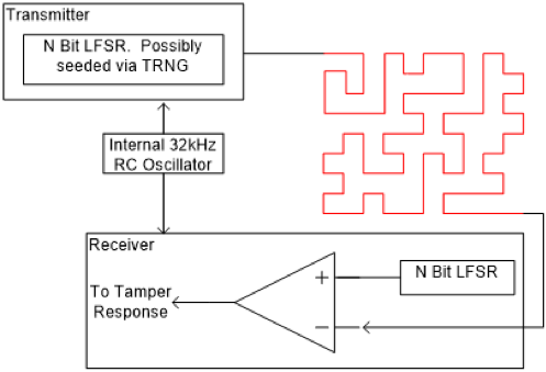
If the active shield is compromised through microprobing or other physical attack, the pulse received will not match the expected signal, and a tamper event can be assumed (Figure 1). The action taken in response to this attack can take several forms, such as disabling sections of the IC, resetting the system or even erasing entire sections of memory – all of which would further frustrate the attacker but, more importantly, protect the system’s data and IP.
In order to create an effective defence, the design team should consider what parts of the design need protection and the number of active shields required to achieve that. This will extend to determining where each shield should be positioned to cover each region of data or IP to be protected.
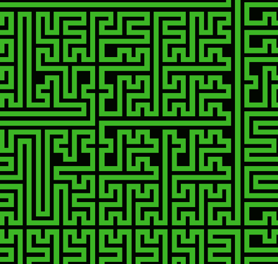
In defining the shield, it is important that the area to be protected is completely filled with the trace and that the trace itself follows a random pattern that could not be guessed or deduced by a potential attacker (Figure 2).
Summary
The applications for active shields in military and defence applications are obvious. However, with many commercial applications containing significant amounts of IP as well as sensitive data, the need for protection is higher than ever before.
While software techniques such as encryption can offer some protection, an active shield placed over sensitive areas enables the IC to detect the presence of a tampering attack and to take measures to protect the design and data, including immediate deletion of all sensitive information where this is considered to be the best defence.
The beauty of the active shield lies in its simplicity while its strength lies in its truly random layout. ON Semiconductor’s ‘Random Orthogonal Plane Filling Curve’ allows designers to create truly random layouts based on a few simple parameters with the added benefit of a processable DEF file as the output.
To learn more about this approach, download ON Semiconductor’s anti-tamper active shield white paper.


