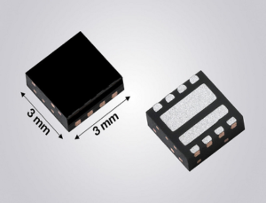
40 V MOSFET Half-Bridge Power Stage Offers Best in Class RDS(ON) and FOM to Increase Power Density and Efficiency
Space-Saving Device Features Maximum RDS(ON) Down to 8.05 mΩ and Qg of 6.5 nC in Compact PowerPAIR® 3x3S Package
Vishay Intertechnology introduced a new Integrated 40 V n-channel MOSFET half bridge power stage, a Space-Saving Device delivering increased power density and efficiency for white goods and industrial, medical, and telecom applications. Integrating high side and low side MOSFETs in one compact PowerPAIR® 3.3 mm by 3.3 mm package, the Vishay Siliconix SiZ240DT provides best in class on-resistance and on-resistance times gate charge — a key figure of merit (FOM) for MOSFETs used in power conversion applications.
The two TrenchFET® MOSFETs in the SiZ240DT are internally connected in a half-bridge configuration. The SiZ240DT’s Channel 1 MOSFET, which is typically used as the control switch in a synchronous buck converter, provides maximum on-resistance of 8.05 mΩ at 10 V and 12.25 mΩ at 4.5 V. The Channel 2 MOSFET, which is typically a synchronous switch, features on-resistance of 8.41 mΩ at 10 V and 13.30 mΩ at 4.5 V. These values are up to 16 % lower than those of the closest competing products. When combined with low gate charge of 6.9 nC (Channel 1) and 6.5 nC (Channel 2), the resulting on-resistance times gate charge FOM is 14 % lower than the next best device, enabling higher efficiency for fast switching applications.
65 % smaller than dual devices in 6 mm by 5 mm packages, the dual MOSFET released today is one of the most compact integrated products on the market. It provides designers with a space-saving solution for motor control in vacuum cleaners, drones, power tools, home / office automation, and non-implantable medical devices, in addition to half-bridge power stages for synchronous buck DC/DC converters, wireless chargers, and switch-mode power supplies in telecom equipment and servers.
The integrated MOSFET features a wire-free internal construction that minimizes parasitic inductance to enable high frequency switching and thus reduce the size of magnetics and final designs. Its optimized Qgd / Qgs ratio reduces noise to further enhance the device’s switching characteristics. The SiZ240DT is 100 % Rg- and UIS-tested, RoHS-compliant, and halogen-free.


