


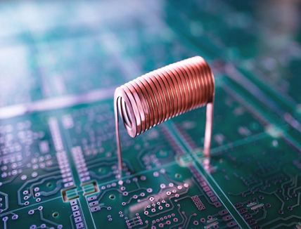
Printed circuit sheets are all over! You most likely utilize one more frequently than you may suspect. However, what precisely would they say they are, and how would they work? PCB’S commonly known as Printed Circuit Boards, are tiny boards made up of thick insulating material.
Do you know? It is coated using a protected material with a covered metal surface in some cases on both the top and base. Little engravings are made in the metal, which permits pathways and different metal segments for power to go through various elements. Even if you are a PCB master, it doesn’t mean you know everything about PCBs. Here, in this article, I will guide you with some of the unknown exciting facts about PCB’s that you might not be aware of!
1. Why is PCB Green in Color?
Have you ever thought why every PCB you go through is of dark solid green color? You certainly might have! This is the most frequently asked question we come through! But, in reality, the board itself is brown and green in color that you often go through is the layer of its solder mask. And also, it doesn’t necessarily have to be green, but most are! Some researchers have a theory that some old American Military used it, and from then, it started to spread.
Some PCB manufacturers found out that the green initially developed from the resins and hardeners used. Also, the laminates used in PCB’s have consisted of green layouts. Even many scientists claim that green color catches the human eye the most! Therefore, the green color has been used for a long time, but many PCB manufacturing companies allow you to choose various vivid color options.
2. Who discovered PCB’S and When?
Paul Eisler, an Austrian creator, is credited with the development of the PCB. However, Eisler is given kudos for the creation, which eventually prompted the development dates as far back as the 1890s. In Austria, Paul found out about the utilization of printing innovation. He needed to know whether it was conceivable to utilize the printing procedure to set out all segments in an insulating base rather than interfacing them physically with wires.
In 1936, Eisler was chipping away at a radio when he previously created the PCB. They didn’t take off and see mass use until the 1950s. However, their popularity has developed altogether from that point!
3. PCB’s are Everywhere Around Us!
Yes, you heard it right! They are almost everywhere around us. Today, practically every electronic machine that you use consistently contains a PCB of some sort. PCs, printers, phones, advanced tickers, microwaves, TVs, sound systems—the rundown goes on! PCBs are essential to such an extent that you presumably don’t understand that you are utilizing a gadget with one more often than you can! The explanation is that they save energy and space and is widely used in many applications.
4. How are PCB’s designed?
In PCB manufacturing, the first thing you need to do is make a complete layout design. CAD, i.e., Computer-Aided Design, usually performs this task. Many prototypes PCB manufacturing uses CAD projects to plan both the schematic and the PCB Prototype creation. It permits the board configuration to be tried, watching all the traces are appropriately associated before the PCBs are genuinely made.
5. What do you understand by the term “SMT’?
You must have heard this term before. Haven’t you? The term SMT usually is used in context to PCB manufacturing. Many prototype PCB manufacturing companies use the term very often in PCB Prototype service. SMT is the acronym used for Surface Mount Technology.
It is a method that utilizes programmed hardware to attach segments onto the Printed Circuit Board. It is one of the most regularly used strategies in PCB manufacturing. Initially, the through-opening approach was utilized in assembling, but it had numerous blunders as SMT replaced it after some time.
6. No Wiring Attached?
You might be knowing the fact that mostly all electronic devices use wires as a mode of transmitting energy. However, this isn’t the case in PCB Assembly. PCB uses traces of copper instead of traditional cables for the transportation of electrons. Too much extra usage of wires can take up a lot of space, and using copper traces will make PCB look smaller.
Many PCB Prototype Manufacturers claim that PCB is made using through-hole technology because copper traces can easily pass through the circuit board hole.
7. Different types of PCB’s
There is an assortment of PCB types.
Printed circuit sheets aren’t all very similar. There are a few sorts of circuit sheets accessible, and every one of them has its properties that are reasonable for specific assignments. A few varieties of sheets might be more fit for low-execution gadgets, which implies that they are less expensive and simpler to make.
Though different sorts of sheets might be more fit to high power gadgets yet will be more costly to create. Here are the various kinds of sheets: Single-sided, twofold sided, multi-layered, adaptable, unbending, adaptable inflexible, and metal-supported.
8. Silkscreens
Have you ever pondered the white etchings you have seen on top of the green PCB patch veil? This is the silkscreen, and it is utilized on the segment side of the circuit board to distinguish segments and other PCB data. The white content can be silk screen printed, which is where it gets its name; however, it is progressively published utilizing computerized ink-stream printers.
9. They’re dependent upon laws (Ohm’s Law)
The principles of physical science carefully oversee over printed circuit sheets. The most popular of these among electrical architects is Ohm’s Law. Ohm’s Law directs the connection between current, opposition, and voltage. As stated right, the guideline electrical flow is relative to voltage and conversely corresponding to obstruction. These laws direct how we can plan and fabricate our PCBs, so an electrical architect must comprehend their suggestions.
10. Innovation is continually evolving.
PCBs have changed massively since the time of Paul Eisler in 1936. They’re such a lot more modest, quicker, and more productive to fabricate. Anyway, PCB innovation is continually advancing. At present, researchers are chipping away at making biodegradable PCBs. Also, the advancement of the material ‘graphene’ could change the manners by which our hardware works. PCBs are rarely static; the innovation is continually creating.
Conclusion!
By now, you must have known some of the fascinating facts about PCB’S that you didn’t know. I hope this article gives you a clear idea about the information on PCB and their unknown facts. This article will also help you clear all your doubts regarding the principle of PCB and its applications.
Author Bio:
Laura Stevens works as a digital marketing manager at PCBGOGO. PCBGOGO manufactures high-quality PCBs and provides the best PCB assembly services that are affordable and effective. In her free time, she writes informational blogs and articles that aim at helping people.
“For more information about PCB, you can refer to Victory PCB. It is a China PCB supplier which specializes in the production of printed circuit boards.
With advanced PCB production and testing equipment, and well-found quality system to monitor throughout the whole manufacturing to assembly,
we can ensure the stable and excellent quality of the production process to meet customers’ requirements”.


