


Question:
How can you easily select the right coil for high voltage inverting buck-boost topologies?
Answer:
By using simplified duty cycle equations to plot the coil current ripple vs. the input voltage for the output voltage of our circuit, then validating the findings with LTspice®.
Introduction
A variety of topologies can be considered for applications that require the generation of a negative voltage rail, as illustrated in the article “The Art of Generating Negative Voltages.”1 However, if the absolute voltage at the input and/or output can exceed 24 V and the required output current can reach a few amperes, the charge pump and the negative LDO regulator are to be discarded due to their low current capability, whereas the size taken by their magnetic components causes the flyback and the Ćuk converter solutions to become quite cumbersome. As a result, under such conditions, the inverting buck-boost provides the best compromise between high efficiency and small form factor.
However, to reap these benefits, the operation of the inverting buck-boost topology under high voltage conditions must be fully understood. Before diving into such details, we will begin with a brief review of the inverting buck-boost topology. Then, we will compare the critical current paths of the inverting buck-boost, buck, and boost topologies.
The Three Basic Nonisolated Topologies
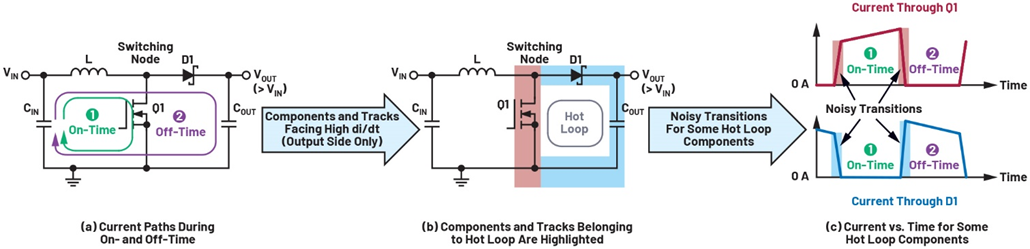
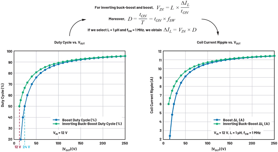
The inverting buck-boost belongs to the three basic nonisolated switching topologies. These topologies all consist of a control transistor (usually a MOSFET), a diode (which can be a Schottky diode or an active diode—the synchronous MOSFET), and a power inductor as the energy storage element. The common connection between those three elements is referred to as the switching node. The positioning of the power inductor with regards to the switching node determines the topology.
If the coil is located between the switching node and the output, we obtain the DC-to-DC buck converter, which we simply call buck in the rest of this article. Alternatively, positioning the coil between the input and switching node creates the DC-to-DC boost converter, referred to as boost here. Finally, the DC-to-DC inverting buck-boost consists of placing the coil between the switching node and ground (GND).
During each switching period and even in continuous conduction mode (CCM), all three topologies include components and PCB traces that are facing fast changes in current, leading to the noisy transitions highlighted in Figure 1c, Figure 2c, and Figure 3c. By keeping the hot loop small, the electromagnetic interference (EMI) radiated by the circuit can be reduced. At this stage, it is worth mentioning that the hot loop is not necessarily a physical loop through which the current circulates. Indeed, for the respective loops highlighted in Figure 1, Figure 2, and Figure 3, the sharp current transitions do not occur in the same direction for the components and tracks highlighted in red and blue that form the hot loop.
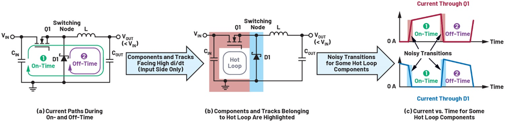
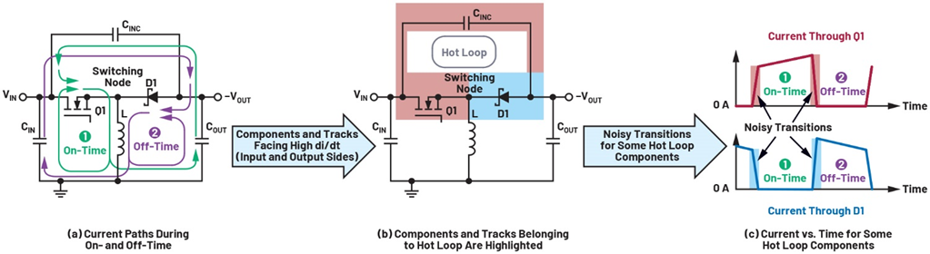
For the inverting buck-boost operating in CCM represented in Figure 3, the hot loop consists of CINC, Q1, and D1. Compared with the hot loop of the buck and boost topologies, the hot loop of the inverting buck-boost contains components located both on the input and output sides. Among these components, the reverse recovery of the diode (or body diode if using a synchronous MOSFET) when the control MOSFET turns on generates the highest di/dt and EMI. Since a thorough layout concept is needed to contain the radiated EMI from these two sides, the last thing you want is to create additional radiated EMI through excessive coil current ripple by underestimating the required inductance of the inverting buck-boost under high input and/or output voltage conditions. This risk exists for engineers who rely on their familiarity with the boost topology to size the inductance of their inverting buck-boost circuit, as we now see by comparing both topologies.
Design Considerations of Inverting Buck-Boost with High Voltages
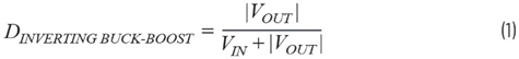
Both the boost and the inverting buck-boost can generate an absolute output voltage whose amplitude is higher than the input voltage. There are, however, relevant differences between both topologies that can be highlighted with the help of their respective duty cycles in CCM, provided in Equation 1 and Equation 2. Please note that these are first-order approximations that do not consider effects such as the voltage drops through Schottky diodes and power MOSFETs.
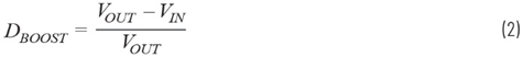
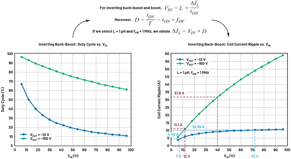
The first-order approximation for the variation of these duty cycles vs. |VOUT| and with VIN = 12 V is plotted on the left side of Figure 4. Moreover, assuming in both cases a switching frequency (fSW) of 1 MHz and an inductance of 1 µH for the power coil, the variation of the coil current ripple vs. VOUT was obtained on the right side of Figure 4.
We observe in Figure 4 that the duty cycle of an inverting buck-boost will exceed 50% from a much lower |VOUT| than the boost: 12 V and 24 V, respectively. It can be understood by referring to Figure 5.
In the case of the boost, the inductor is in the path between input and output. Therefore, the voltage through the power inductor (VL) adds up to VIN to provide the required VOUT. However, for the inverting buck-boost, VL is the sole contributor to the achieved output voltage. On that occasion, the power inductor must provide much more energy to the output, which explains why the duty cycle already reaches 50% for a much lower |VOUT|.
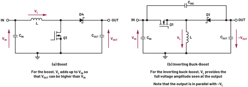
We can reformulate this observation by stating that, as the ratio |VOUT|/VIN decreases, the duty cycle drops much slower for the inverting buck-boost as for the boost. This is an important fact to consider during design, and its impact can be better understood by referring to Figure 6, where the first-order approximation of the duty cycle and coil current ripple are redrawn, but this time vs. VIN.
As demonstrated in Figure 6, the coil current ripple (ΔIL) is proportional to VIN and D. In the case of the boost, as VIN becomes higher than half of VOUT, the duty cycle decreases faster than VIN increases, going from 50% at VIN = 24 V to a quarter of this value at VIN = 42 V for the blue curve on the left graph of Figure 6. Consequently, ΔIL decreases quickly for VIN above 24 V for the boost on the right graph of Figure 6.
However, for the inverting buck-boost, we previously saw in Figure 4 that D decreases very slowly when |VOUT|/VIN decreases or, said differently, when VIN increases for a fixed |VOUT|. This can be seen for the green curve on the left graph of Figure 6, where the duty cycle loses only 25% when VIN increases by 62.5% from 48 V to 78 V. Since the decrease in D does not compensate for the increase in VIN, the coil current ripple increases significantly with VIN, as illustrated by the green curve on the right graph of Figure 6.
Overall, the higher coil current ripple potentially faced under high voltage conditions by the inverting buck-boost compared with the boost explains why the former topology requires higher coil values if operating at the same fSW. Let’s use this knowledge in a concrete case with the help of Figure 7, which is, as well, based on first-order approximations.
Application with Wide Input Voltage Range and High Output Current
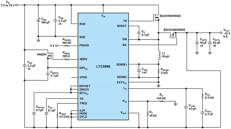
Let’s consider an application with VIN = 7 V to 72 V and VOUT = –12 V at 5 A. Given the high output current, we opt for a synchronous controller (LTC3896) to achieve high efficiency.
Selecting the Inductance
When operating the LTC3896 in CCM, it is recommended to keep ΔIL between 30% and 70% of IOUT,MAX, which is 5 A for our example. Consequently, we want to design for ΔIL between 1.5 A and 3.5 A over our whole input voltage range. Moreover, staying within this recommended range between 30% and 70% of IOUT,MAX means that we can only afford a ratio of up to 2.33—that is, 70% divided by 30%—between the highest and lowest current ripple over our input voltage range. This is not a trivial task for a topology such as the inverting buck-boost where ΔIL varies significantly with VIN, as previously observed.
Referring to Figure 7, when using fSW = 1 MHz and L = 1 µH, the coil current ripple would vary between 4.42 A and 10.29 A, which is far too much. In order to position the lowest ΔIL to our recommended lower limit of 1.5 A or 30% of IOUT,MAX, we need to reduce the existing value of 4.42 A by a factor of three. This can be achieved by setting fSW to 300 kHz with a 47.5 kΩ resistor at the FREQ pin and selecting a 10 µH inductance. Indeed, this scales down ΔIL by (1 µH × 1 MHz)/(300 kHz × 10 µH) = 1/3.
Thanks to this scaling, the coil current ripple (ΔIL) should now vary between about 1.5 A and 3.4 A (between 30% and 68% of IOUT,MAX) over the whole input voltage range, which is just within the recommended range. We obtain the circuit provided on the last page of the LTC3896 data sheet, which is reproduced in Figure 8.
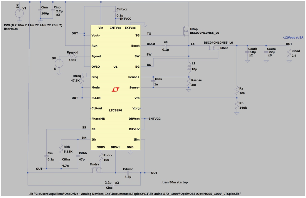
Validating Our Inductance Selection with LTspice
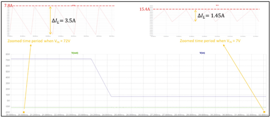
Regarding the coil current ripple, more accurate values can be obtained by simulating the same LTC3896 circuit with LTspice, as demonstrated in Figure 9. In Figure 10, ΔIL equals about 1.45 A and 3.5 A, respectively, at VIN = 7 V and 72 V, which is consistent with the first-order approximation values previously extracted with the help of Figure 7 and the scaling of the fSW and L. Please note that the coil current probed in Figure 10 is considered positive when flowing towards RSENSE.
An additional benefit of the LTspice simulation is to determine the peak coil current faced during operation, which is obtained at the lowest input voltage of 7 V. As seen in Figure 10, our application will face a peak coil current close to 15.4 A. By knowing this value, a power inductor with a high enough current rating can be selected.
Designing with Even Higher Output Voltages
If we return to Figure 7, the current ripple values were also provided for a hypothetical case with a VIN range from 12 V to 40 V and a VOUT equal to –150 V.
The first remark is that the current ripple is getting significantly higher for higher VOUT when keeping the same fSW and L. Such high ΔIL are often unacceptable, therefore, we would have to apply a higher scaling down factor compared with the previous example, which means a higher inductance for the same fSW.
The second remark refers to the variation of ΔIL over the whole input voltage range. For the previous example with VOUT = –12 V, ΔIL was only increasing by about 2.33 from lowest to highest ripple with the input voltage increasing more than tenfold. For the present case with VOUT = –150 V, ΔIL already increases by 2.85 from lowest to highest current ripple, and this despite the input voltage only increasing by a factor 3.33 from 12 V to 40 V.
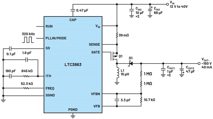
Luckily, such challenges only exist in CCM. When in discontinuous conduction mode (DCM), limitations such as 30% to 70% of IOUT(MAX) no longer apply. It would anyway be too strenuous to convert VIN = 12 V to VOUT = –150 V at IOUT(MAX) = 5 A in a single step. In any case, when such voltage conversions are required, the output current requirement is generally low, meaning that we operate in DCM. This is, for example, the case for the circuit on the last page of the LTC3863 data sheet, reproduced in Figure 11.
Due to the low DC currents, using a nonsynchronous controller such as the LTC3863 was good enough to provide an acceptable efficiency under these conditions. In the case of this LTC3863 design in DCM, the LTC3863 circuit provided with LTspice is a nice tool to optimize the coil selection.
Conclusion
The hot loop of the inverting buck-boost topology includes components located both on the input and output sides, making its layout more difficult to implement than the buck and the boost topology.
Although there are some analogies to the boost, the inverting buck-boost faces much more current ripple under similar application conditions because its coil constitutes the only source of energy to the output (if we ignore the output capacitance).
For inverting buck-boost applications with high input and/or output voltages, the coil current ripple is potentially even higher. To contain it, higher inductance values are used compared with the boost topology. A practical example was used to demonstrate how to quickly scale the inductance based on the application conditions.
Reference
1Dostal, Frederik. “The Art of Generating Negative Voltages.” Power Systems Design, January 2016.

About the Author
Olivier Guillemant is a central applications engineer at Analog Devices in Munich, Germany. He provides design support for the Power by Linear portfolio for European broad market customers. He has held various power application positions since 2000 and joined ADI in 2021. He received his M.Sc. in electronics and telecommunications from University of Lille, France.


