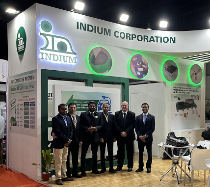
Indium Corporation, the global manufacturer and supplier of materials for electronics and semiconductor assembly, thermal management, showcased its innovative products at Productronica India. In a conversation with our editor Pratibha Rawat, Jonas Sjoberg, Associate Director for Global Technical Service & Application Engineering and Damian Santhanasamy, Senior Country Sales Manager, Malaysia talk about the Indium Corporation’s solutions for the Indian market and how they support the supply chain issue in critical situations. They also addressed the challenges, associated with solder deposition, SiP application and thermal management.
Mobile assembly, manufacturing, and 5G are the hottest topics in India. What is Indium Corporation offering for these segments related to the Indian market?
Jonas Sjoberg: We are seeing a big trend of miniaturization in mobile devices. Components are getting smaller, which are driving the need for different and finer powders. The powder size for specific solder paste applications is an important consideration. For instance, finer powders can screen print smaller deposits of solder paste. We are offering new powders and new fluxes that we blend with the powders.
We have launched a few new materials. From our point of view, the material selection typically relates primarily to solder paste materials. Along with the solder paste materials, we also offer overall knowledge about other processes to help our customers find the right solution.
Solder preforms are another offering that we use for mobile die-attach, which are quite useful in 4G. However, for 5G, the use of preforms is limited as 5G technology uses mainly solder paste.
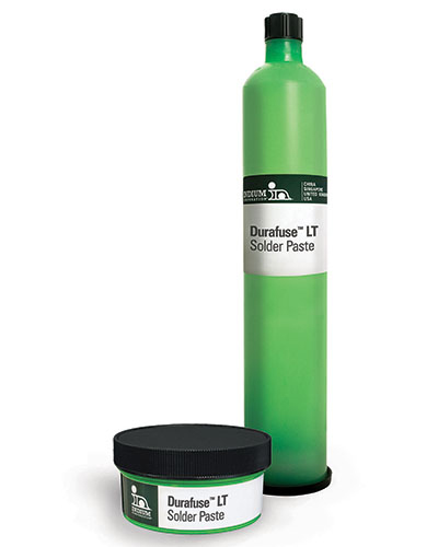
As mentioned earlier, components are getting smaller and smaller; this is the same with infrastructure. One of the materials that we promoted here at Productronica is Durafuse™ LT. This product is originally a low-temperature alloy. We can reflow it at 200° C, but it can also be reflowed at 265°C. If you look at some of the automotive power products or infrastructure, the boards are large with a mix of small and very large components; not everything heats up evenly. Many components and boards aren’t supposed to be exposed to temperatures above 255‒260°C. Durafuse™ LT is designed to provide high-reliability in low-temperature applications that require a reflow temperature below 210°C.
Apart from soldering material, there are many variables that come into play and high reliability is one of them, whether for mobile devices or infrastructure. Different mobile suppliers ask for different thermocycling requirements. For instance, one supplier might ask for a thermocycling requirement of 0°C to 85°C while another mobile supplier might ask for -40°C to 100°C. Because we have an overall understanding from both the sales point of view and the tech point of view, this enables us to give customers the right material that they are looking for.
We have a solder paste which is not used so differently between 4G and 5G applications in many cases. But one thing that we’ve seen, especially here in India, many infrastructure products are using ICT testing. This means that the flux we use will be different when compared to the flux that we use for mobile devices.
A strength that we’re offering as a company, which is different from our competitors, is that many of our team members, both in India and in China, come from a mobile device background.
Discrete components become smaller and create challenges for solder deposition. What are Indium Corporation’s offerings for this issue?
Jonas Sjoberg: In today’s world with electronics continuing to get smaller and smaller, the size of the solder powder used in a solder paste matters because the size of the solder powder affects the solder paste performance. Solder powder types can range from Type 3 (the largest) down to Type 7 (the smallest).
In India, sometimes we see the usage of Type 4 powder and sometimes Type 3 powder as it is the cheapest, but as Type 4 powder has increased in usage, its price has gone up. However, with smaller features required especially for mobile and automotive, Type 5 powder is the preferred choice, which has a different distribution. For example, instead of being able to print minimum apertures of 250 microns, we can go down to about 200 microns. But by changing the powder type, we can go from a powder size of 20‒38 microns (Type 4) to 15‒25 microns, as seen in Type 5.
SiP has numerous benefits and heterogeneous integration has made it the first choice for engineers. What are the factors engineers must consider while selecting material for SiP applications?
Jonas Sjoberg: Proper design development is the key factor engineers must consider first. If you don’t have a good design, the material doesn’t matter.
One of the key features of SiP is the flux which can work with fine powders such as Type 6 or Type 7. Flux must be a bit more active than what you use for normal PCBA manufacturing, and it also must print well. If it doesn’t print well, it won’t pass the SPI inspection. So, material that prints well is the key consideration for SiP. Once you have that, you can start looking into avoiding spattering, voiding, and bridging as well. But printing, I think, is key when working with SiP materials.
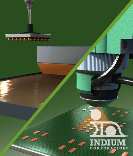
As seen in semiconductors, when the complexity of SiP increases, cleanability is very important. Some SiP modules have a shield mounted on top, but some of them need to be cleaned and then moulded. Engineers must see whether the package is shielded or moulded. Do you need a water-wash material or a no-clean material? Ideally, you don’t want to wash it, but in some cases, you must wash it. If there is a SiP module flip-chip and if it is a shielded application, one can use no-clean solder pastes for the passive component and then use ultra-low residue flip-chip fluxes.
We must work with the customer on both the PCBA base and components within the package. A material supplier cannot just be a material supplier; they must have a full understanding of the design itself and should fulfil reliability requirements.
Indium Corporation has expanded over the years into a variety of different markets. What are the key markets and technologies for the Asian region?
Damian Santhanasamy: In Asia, mobile devices, automotive, and infrastructure, such as 5G, are our key markets. We also serve various other markets such as defence, medical, MEMS, PCBA, and power modules.
Some applications have very high requirements, such as in defence, while mobile devices and automotive markets can share some of the same solutions, so applications and solutions will differ.
How are wide band gap semiconductors, SiC, and GaN changing packaging technology?
Damian Santhanasamy: If it is referred to as die technology, we are working with SiC, but GaN is not that popular. As you move towards higher densities, SiC sees more traction and we have materials for SiC.
Thermal management is a key feature of emerging technologies. How is Indium Corporation developing materials science to address these challenges?
Damian Santhanasamy: If you consider the mobile phone space, we solder at a thermal conductivity of 35W/mK, but we are also in the range of a data computing cloud service where a higher thermal conductivity of 86W/mK is needed. Indium Corporation has a range of materials and solutions for thermal management needs from the lower to the higher side. For thermal management requirements, we offer indium foil and Heat-Spring® materials. Our R&D never stops bringing new materials to answer customer requirements. We also have different shapes and sizes of preforms which enable high thermal conductivity and high performance from the chips.
We always listen to our customers and speak “from one engineer to another.” We even consider the entire package to see what kind of thermal conductivity solution is needed.
After government announcements related to fabs, displays, and packaging, what future does Indium Corporation see in India?
Damian Santhanasamy: We are looking two years ahead, as Indium Corporation has been successful so far in the semiconductor space. We have been supplying a lot of soldering material fluxes in countries such as Korea, Japan, Asia, and China for die-attach MOSFET, isolated gate bipolar transistors, IGBTS, and so on. We have been quite successful, and we are looking forward to sharing that with India as well.
Jonas Sjoberg: We have yet to see what types of applications emerge as the semiconductor space is very wide. If it is wafer fab or assembly or packaging, we are getting more involved in some of the organizations here in India and IESA is one of them that we’re looking into.
What are the major challenges you see for Indian customers and engineers?
Jonas Sjoberg: I travel all over the world, and I have missed coming to India for the past three years. The questions that the Indian engineers have are very valid, and they’re very curious to get to know more. We had a few meetings this week, and last week a meeting that was scheduled for one hour ended up being four hours. Indium Corporation has the experience to investigate the root cause of problems and help solve the concerns that the engineers have
Damian Santhanasamy: Our technology sharing is not one-way—it is two-way—so we answer basic questions and elaborate as we go along as the talk is from both sides. We always look for collaboration to help us learn and provide the right solution.
How has Indium Corporation continued to support India and deal with supply chain issues?
Damian Santhanasamy: In terms of the supply chain, we have two backups for India; one is in Singapore and the other is in Penang, Malaysia, which is our new facility. We have two factories supporting our Chennai facility in India. As a business in India grows, we also need to accelerate our footprint.
Jonas Sjoberg: Indium Corporation’s business continuity plan shows that we are positioned everywhere. Due to our locations, we can move production quickly, so we have not seen any big impact. We do have plans for the future expansion in India.


