


Objective
This lab activity is an introduction to Phase-Locked Loop (PLL). The Phase-Locked Loop circuit has several important applications, such as signal modulation/demodulation (mainly frequency and phase modulation), synchronization, clock, and data recovery, as well as frequency multiplication and synthesis. In this activity, you will set up a simple Phase-Locked Loop circuit to gain basic understanding of PLL operation.
Background
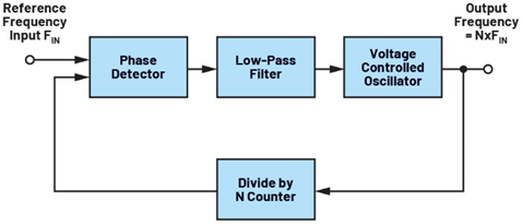
A Phase-Locked Loop is a feedback system that acts to adjust or lock the phase difference between the output of a voltage-controlled oscillator (VCO) and an input reference signal as shown in Figure 1. A VCO is an oscillator whose output frequency is a function of some input control voltage. Generally, when a VCO is used in a feedback loop like a Phase-Locked Loop, the voltage to frequency transfer function must at least be monotonic. A special case of a VCO is the voltage-to-frequency converter (VFC) where the voltage/frequency characteristic is linear. The divide factor N of the frequency divider in the feedback loop is generally an integer number including 1, which is the same as having no divider or a direct connection from the VCO output to the input of the phase detector.
Phase-Locked Loop are the subject of many in-depth books and discussions and are far too complex to deal with exhaustively in these few pages. Additional reading material is linked at the end of this lab.
Materials
- ADALM2000 Active Learning Module
- Solderless breadboard
- Jumper wires
- One 2.2 kΩ resistor
- One 47 kΩ resistor
- One 10 kΩ resistor
- One 4.7 nF capacitor (marked 472)
- One 100 pF capacitor (marked 101)
- One CD4007 CMOS array
- Two ZVN2110A NMOS transistors
- Two ZVP2110A PMOS transistors
- One AD654 VFC
- One 9 V battery (with connector)
Step 1 Directions
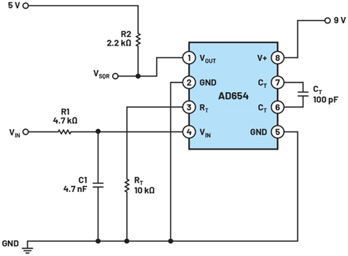
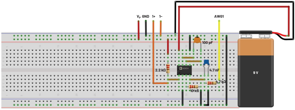
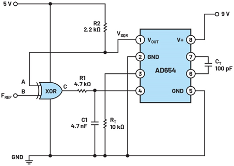
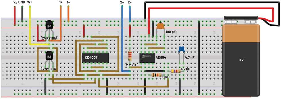
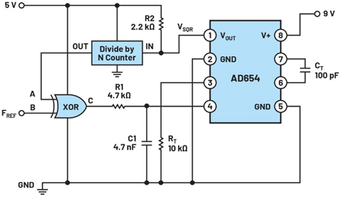
On your solderless breadboard, first construct the VFC circuit based on the AD654 shown in Figure 2. Build the circuit to one side of your breadboard to leave space for the other parts of the Phase-Locked Loop we will be adding in later steps of this lab activity. The control voltage is applied through a single-pole low-pass filter consisting of R1 and C1. This is equivalent to the low-pass filter block that feeds the VCO block in Figure 1.
Hardware Setup
Turn on the fixed 5 V power supply and connect the 9 V battery to your circuit. Connect AWG1 output to VIN as shown in Figure 2. Configure AWG1 as a DC source and set it to 2.5 V initially. Connect scope channel input CH1+ to the VSQR output as shown in Figure 2. You should ground the CH1– input as well.
Procedure
Using the AWG 1 DC offset controls, adjust the voltage at VIN from 1 V to 4 V while observing the frequency of the VFC output at VSQR. Use the frequency measurement feature on the scope control screen to do this. Rt and Ct in Figure 2 set the nominal output frequency of the VFC according to Equation 1.
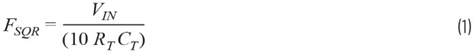
For example, with VIN set in the middle of the range at 2.5 V and the given Rt Ct values (2.5/(10 × 10 kΩ × 100 pF)), the output frequency should be near 250 kHz. Verify that your measurements agree with this value. If not, then recheck your circuit connections and component values.

Step 2 Directions
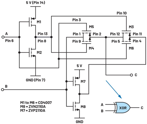
Next add the XOR gate phase detector circuit from the previous activity on your breadboard as shown in Figure 5. After constructing the XOR gate, connect it to the V to F circuit as shown in Figure 6 to make the complete Phase-Locked Loop. Be sure to turn off the 5 V power supply and disconnect the 9 V battery before making any additions to your circuit.
Hardware Setup
Turn on the fixed 5 V power supply and connect the 9 V battery to your circuit. Connect AWG1 output to FREF as shown in Figure 4. Configure AWG1 as a square wave with an amplitude of 5 V peak-to-peak and an offset of 2.5 V (0 V to 5 V swing) and initially set the frequency to what you measured in Step 1 when VIN was set to 2.5 V (should be around 250 kHz). Connect scope channel input CH1+ to the FREF input and scope channel CH2+ to VSQR output as shown in Figure 6. You should ground the CH1– and CH2– inputs as well. Set the scope to trigger off the rising edge of Channel 1 (the FREF signal).
Procedure
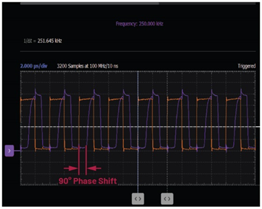
With FREF set to the frequency corresponding to a control voltage of 2.5 V on Pin 4 of the AD654, the output frequency seen at VSQR should be locked to the input reference frequency FREF. On the scope screen, you should see that the two square waves are stable (that is, locked to each other) and VSQR is shifted approximately 90° with respect to FREF. Remember that the filtered output of the XOR phase detector will be at one-half of its output range or about 2.5 V when its two inputs are 90° apart in phase.
Increase and decrease the reference frequency, FREF, in small increments to determine the minimum and maximum frequency the Phase-Locked Loop will lock to. Note the relative phase difference between FREF and VSQR while you are changing the frequency of the reference input. While doing this, measure the filtered DC control voltage seen on Pin 4 of the AD654 and compare these readings to what you measured in Step 1 when sweeping the DC control voltage of the VFC.
Connect Scope Channel 2 to the output of the XOR gate at Point C in Figure 6. Compare the square wave you see to the inputs of the XOR Gate A (VSQR) and Gate B (FREF). How does the shape of the waveform at C change when the Phase-Locked Loop is locked to the minimum and maximum lock frequency vs. the frequency in the center of the lock range?
Bonus Step 3 Directions
The simple Phase-Locked Loop circuit of Figure 6 is not very interesting in that the output signal is just a phase shifted version of the input signal. If we insert a digital divider block in the feedback path from the VFC output to the phase detector input as we saw back in Figure 1, then the output signal will be at a higher multiplied frequency. Using any digital divider IC you might have available such as a CD4020, CD4040, CD4060, or even SN7490 (just about any divider IC will do), open the connection to XOR Input A and insert the divider block as shown in Figure 9.
Depending on the divide factor N of the divider you build, you will need to change the FREF input frequency by that amount. For example, with N = 8, if FREF was 250 kHz before, the new FREF would be 250/8 or 31.25 kHz. The frequency of the pulses at the output of the XOR gate phase detector will also be eight times lower.
For further reading: analog.com/media/en/training-seminars/tutorials/MT-086.pdf
Question
1. Can you name several real-life applications of the Phase-Locked Loop circuits?
You can find the answer at the StudentZone blog.
About the Author

Antoniu Miclaus is a system applications engineer at Analog Devices, where he works on ADI academic programs, as well as embedded software for Circuits from the Lab®, QA automation, and process management. He started working at ADI in February 2017 in Cluj-Napoca, Romania. He is currently an M.Sc. student in the software engineering master’s program at Babes-Bolyai University and he has a B.Eng. in electronics and telecommunications from Technical University of Cluj-Napoca.
About the Author

Doug Mercer received his B.S.E.E. degree from Rensselaer Polytechnic Institute (RPI) in 1977. Since joining Analog Devices in 1977, he has contributed directly or indirectly to more than 30 data converter products and holds 13 patents. He was appointed to the position of ADI Fellow in 1995. In 2009, he transitioned from full-time work and has continued consulting at ADI as a fellow emeritus contributing to the Active Learning Program. In 2016, he was named engineer in residence within the ECSE department at RPI.


")


