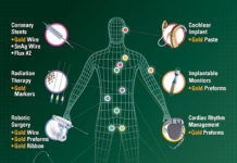
Medical devices aren’t immune to the latest machine learning opportunities, but the existing components don’t always satisfy the new engineering needs, which is why the Page EEPROM series by ST is finding design wins in healthcare. Put simply, the new hybrid memory architecture combines an EEPROM’s robustness and power efficiency with the speed and capacity of flash memory. We currently offer modules with eight times more storage than EEPROM to reach up to 32 Mbits while keeping the write time at about 2 ms, which is about half that of an EEPROM. Let’s thus see what such a module can bring to a highly constrained product like a behind-the-ear (BTE) hearing aid and more.
Constraints today
The case of the hearing aid
A paper funded by the Federal Ministry of Education and Research of Germany and presented at the 48th European Solid-State Circuits Conference in 20221 looked at a modern take on the BTE hearing aid. The researchers used a Bluetooth SoC and a DSP to process audio. The purpose was to create something small enough to be usable in clinical settings over long periods while having the computational capabilities to try new algorithms. The fact that the authors specifically mention the exploration of neural networks as a reason behind their paper further emphasizes the need to bring machine learning to this industry.
Today’s memory limitations
However, the scientists hit a pretty important limitation common to many industries: memory capacity. The researchers used 2.5 MB of memory for data and 375 KB for instructions. The obvious issue is that even the smallest neural networks will need far more than that. However, the increase in capacity cannot result in a compromise in robustness or overall power consumption. In this instance, the area behind the ear is a major constraint, and direct contact with the patient’s skin prohibits any increase in heat dissipation. Consequently, a significant bump in memory capacity can’t just come from existing devices but requires a new memory architecture.
Greater capacity also opens the door to new levels of efficiency. In this instance, instead of having external and internal modules, engineers can create one memory pool that can satisfy all their needs. It’s an increasingly common practice in embedded systems because it offers a lot of benefits. Among others, it helps simplify designs, which reduces development times and the bill of materials. It also helps optimize memory access for greater performance. Finally, companies significantly lower the risk of shortages or shipping issues since they only need one module. As memory availability can suffer from high volatility, relying on one module simplifies the sourcing and qualification process.
Architectures tomorrow
The need for memory pages
At its simplest, all digital information today takes the form of zeros and ones, and each value is stored in a bit, which represents the most basic unit of computing2. Due to historical reasons, memory structures today take 8 bits to form a byte. In a traditional EEPROM, the architecture provides byte-level precision, which gives unparalleled granularity. However, erasing and writing operations take longer. Additionally, the byte-level architecture of a standard EEPROM means a bigger die. Consequently, it limits the overall capacity possible in a small component, which explains why it is difficult to significantly increase the capacity of traditional EEPROM.
To remedy this, the industry has long since adopted the notion of words, which groups bytes, and pages, which bundle words together. Thanks to this system, a memory controller can erase more cells at once, thus accelerating the process at the cost of the byte-level flexibility. For instance, serial flash traditionally has a page size of 256 bytes. Additionally, the memory is organized in sectors, which is the standard block of memory that the controller can erase at once. In most serial flash of comparable sizes to our Page EEPROM, the sector size is 4 KB. Thanks to this structure, it is possible to create significantly smaller dies. However, engineers lose the flexibility of the byte-level EEPROM.
The need for a hybrid architecture
The Page EEPROM is unique because while it uses 16-byte words and 512-byte pages to improve performance and capacity, it also enables byte-level granularity thanks to a smart page management system. More precisely, the memory controller is capable of byte-level write operations to optimize certain processes like data logging while offering efficient erase and program operations for firmware updates. Consequently, it adopts a hybrid structure to keep the flexibility of a traditional EEPROM while featuring the capacity and speed of flash. The ST architecture also checks a 17-bit error-correcting code (ECC) signature after each word to improve the overall reliability, thus enabling the correction of 2 bits within 16-byte words.
Page EEPROM: Benefits now
Low power consumption of 500 µA
As explained earlier, power consumption is a central issue for many wearables, like BTE hearing aids. In real-world operations, the Page EEPROM needs about 500 µA when reading data, which is about five times less than a serial flash, and its electrical current peak is less than 1 mA, which means fewer passive components. Additionally, ST’s Page EEPROM has a current peak control system to keep the consumption below 3 mA at all times. Comparatively, a serial flash often experiences high current peaks that lead to wide variations in power consumption. As for writing operations, the Page EEPROM needs fewer than 2 mA, which is even less than the 3 mA of some EEPROM.
Concretely, the levels of power consumption afforded by ST’s Page EEPROM mean that engineers can work with smaller batteries and smaller PCBs to fit more space-constrained applications. Indeed, 500 µA when reading data and less than 1 mA in current peak signify that, compared to a serial flash, a designer can either use a much smaller battery or use the same battery for much longer. Additionally, because the smaller current peak means fewer passive components, the PCB can shrink, which also means a bigger battery in the same case or a smaller design altogether. These are critical considerations for BTE hearing aids that were not possible until Page EEPROM.
High data rate of 320 Mbit/s
As explained, the page architecture of ST’s new memory boosts overall performance. Compared to the 20 Mbit/s of a vanilla EEPROM, the Page EEPROM clocks at 320 Mbit/s in read operations. Consequently, a microcontroller can download its firmware from the Page EEPROM in significantly less time. Additionally, our memory includes a Buffer Load feature that can program several pages at the same time, thus bypassing some of the bottlenecks inherent to the SPI protocol. In practical terms, it means that using the buffer load feature can drastically speed up the programming of hundreds of thousands of devices, thus lowering the overall manufacturing costs. The memory access time is also significantly faster for a wake-up time of 30 µs.
High endurance of 500,000 cycles
The Page EEPROM supports 500,000 read-write cycles per page over the full temperature range (from -40 ºC to +105 ºC), which is about five times better than a serial flash. A traditional EEPROM does have a higher endurance, but we’ve also found that current rates are more than acceptable for integrators since the Page EEPROM, just like the standard one, qualified for a cumulated 1 billion cycle over the entire memory capacity. Indeed, since the ST device has more capacity, developers can spread the wear over more cells, thus extending its life. In fact, many medical devices, like hearing aids, already use serial flash successfully. The endurance of our Page EEPROM thus represents an improvement, not a regression.
Next Steps
The best way to get started with an Page EEPROM is to grab our X-NUCLEO-PGEEZ1 expansion board and download the X-CUBE-EEPRMA1 package. The software bundle provides a demo application that uses the board as an external storage solution, thus showcasing how to read and write from it. It is a quick way to learn how to use a single, dual, or quad SPI interface to interact with the Page EEPROM to run a proof-of-concept or test the hybrid architecture. ST also provides technical documentation to understand the memory architecture better or be familiar with cycling endurance, among other things.
For more information visit: https://blog.st.com/page-eeprom/


