


Next-Gen Chip Printing:
The relentless pursuit of miniaturization in semiconductor manufacturing has been guided by the evolving mastery of light — the very essence of lithography. From the early days of dry lithography, where patterns were projected through air, to the sophisticated immersion techniques that leveraged liquid interfaces for enhanced resolution, each innovation marked a pivotal leap in chip precision. As technology nodes shrank further, the industry transitioned to Extreme Ultraviolet (EUV) and now High-NA EUV systems, pushing the boundaries of optical physics and engineering to print features just a few nanometers wide. This journey through photon pathways not only reflects the ingenuity behind next-generation chip printing but also symbolizes the race to sustain Moore’s Law in an era defined by atomic-scale precision and unprecedented computational demand
Jain emphasizes the intricate physics and engineering behind EUV lithography, along with its impact on next-generation semiconductor scaling, as detailed in “Overview of Extreme Ultraviolet (EUV) Lithography: Shaping Next-Gen Semiconductor Manufacturing” (Electronics Specifier). Taken together, these analyses offer a comprehensive view of how DUV, immersion, and EUV lithography collectively define the photon-driven frontier of nanoscale semiconductor manufacturing.
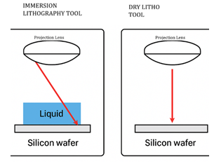
Before exploring the powerful synergy between EUV and DUV lithography and their respective roles across different process nodes, it is important to first grasp the fundamental principles of lithography – the foundational techniques that have shaped the evolution of chip fabrication. In semiconductor lithography, immersion tools and dry tools refer to two different types of photolithography systems used to project circuit patterns onto silicon wafers. The main difference lies in the medium between the lens and the wafer surface – air (dry) or liquid (immersion).
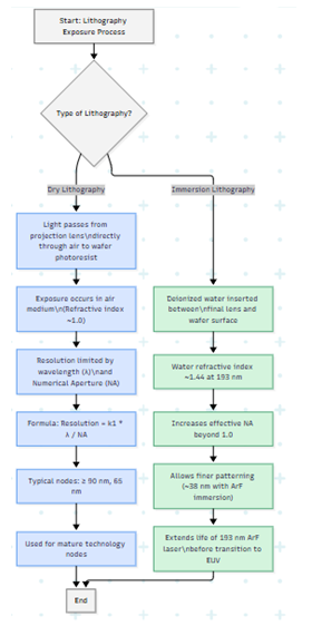
1. Working Principle
In dry lithography, light from the projection lens travels directly through air to expose the wafer photoresist, with resolution limited by the wavelength and numerical aperture of the system. Immersion lithography enhances this process by introducing a thin layer of liquid, typically deionized water, between the lens and wafer. This increases the effective numerical aperture, allowing finer patterning and improved resolution, making it suitable for advanced nodes
2. Resolution and Process Node Impact (Dry vs Immersion)
| Parameter | Dry ArF Tool | ArF Immersion Tool |
| Wavelength (λ) | 193 nm | 193 nm |
| Typical NA | 0.93 | 1.35 |
| Resolution | ~65 nm | ~38 nm |
| Node Application | 90 nm, 65 nm | 45 nm, 32 nm, 28 nm |
3. Advantages & Limitations
| Aspect | Dry Tool | Immersion Tool |
| Pros | Simple system, lower cost, easier maintenance | Higher resolution, extended Moore’s Law scaling, no wavelength change needed |
| Cons | Limited resolution, cannot support advanced nodes | Complex system, requires ultra-clean water, risk of bubbles or defects, higher cost |
4. Technology co-existence
Let’s break down the scope and overlap of EUV and DUV lithography with immersion and dry tools, as these technologies represent distinct, but complementary, phases of lithography evolution.
| Technology | Wavelength | Tool Type | Used For |
| DUV (Deep Ultraviolet) | 248 nm (KrF), 193 nm (ArF) | Dry and Immersion | 90 nm → 28 nm nodes |
| EUV (Extreme Ultraviolet) | 13.5 nm | Vacuum-based (Dry only) | ≤7 nm nodes |
| Lithography Type | Wavelength | Tool Medium | NA Range | Node Range | Status |
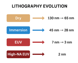
| DUV Dry (ArF/KrF) | 193 / 248 nm | Air | ≤1.0 | 130 → 65 nm | Mature |
| DUV Immersion (ArFi) | 193 nm | Water | ~1.35 | 45 → 14 nm | Widely used |
| EUV (Low-NA) | 13.5 nm | Vacuum | 0.33 | 7 → 3 nm | Production |
| EUV (High-NA) | 13.5 nm | Vacuum | 0.55 | ≤2 nm | Emerging |
5. Why No Immersion in EUV?
- EUV photons are easily absorbed by any medium, including water or air.
- Hence, EUV must operate in vacuum—making it inherently dry.
- All focusing and projection use mirrors, not lenses.
6. Integration of DUV and EUV
Modern fabs use both:
- DUV Immersion → Non-critical or lower layers, alignment, or pattern multiplication.
- EUV → Critical layers (gate, contact, via, metal lines).
Example in a 5 nm process:
- Front-end (fin formation, gate): EUV
- Back-end interconnect: DUV immersion
The views and interpretations expressed here are solely those of the author and do not represent the positions, opinions, or policies of any organization, institution, or professional community.
Final thoughts and Summary
Dry and immersion lithography underpin DUV-based chip fabrication, with dry tools supporting mature nodes (≥90 nm) and immersion methods achieving finer resolutions (~38 nm) by enhancing the effective numerical aperture. EUV lithography, spearheaded by innovators like ASML, pushes this boundary to sub-7 nm nodes, employing 13.5 nm photons for exceptional precision. Photonics lies at the heart of these technologies, governing light propagation, wavelength control, and mask imaging to define nanoscale features. Collectively, DUV, immersion, and EUV photonics-driven lithography enable leading semiconductor companies to sustain Moore’s Law and advance next-generation semiconductor process nodes.
About the Author

Rupal Jain brings a wealth of experience in engineering, program management, and strategic alignment and stands as a distinguished personal in the realm of semiconductor chip manufacturing. She has orchestrated projects spanning the entire spectrum from design conception to final delivery on a global scale, covering regions such as the USA, Taiwan, Singapore, Italy, Malaysia, China, and India. Recognized for her profound expertise, Rupal is celebrated by prestigious certifications such as PMP, CSM, and Lean Six Sigma Black Belt. She holds a master’s in electrical and Electronics Engineering from NTU Singapore, in a joint degree program with TUM Germany. Her contributions have garnered international acclaim, earning her invitations to esteemed publications, media, jury, nominated memberships and coveted awards. Her books “Mastering Project Management: PMP and Agile for Leaders“; “Semiconductor Essentials : A Leader’s Express Reference to Electronic Concepts” and “Advancements in AI and IoT for Chip Manufacturing and Defect Prevention,” shares her valuable insights with the next generation of leaders and engineers.


