Key Highlights:
- An AI-assisted optimization workflow helps shorten design cycle times on TSMC’s compact universal photonic engine (COUPE) platform and strengthens design quality using Ansys optiSLang, Ansys Zemax OpticStudio, and Ansys Lumerical FDTD simulation software
- Ansys HFSS-IC Pro platform is certified for system-on-chip electromagnetic extraction with TSMC’s N5 and N3P process technologies
- Ansys RedHawk-SC and Ansys Totem power integrity platforms are certified for the latest TSMC N3C, N3P, N2P, and A16 process technology releases
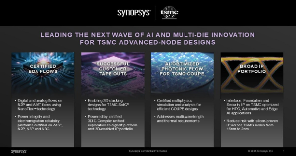
Synopsys, Inc., announced TSMC has certified the Ansys portfolio of simulation and analysis solutions, enabling accurate final checks on chip designs targeted for TSMC’s most advanced manufacturing processes including TSMC N3C, N3P, N2P, and A16. The companies also collaborated on an AI-assisted design flow for the TSMC-COUPE platform. Together, Synopsys and TSMC empower customers to effectively design chips for a range of applications including AI acceleration, high-speed communications, and advanced computing.
Multiphysics and AI-Driven Photonics Design Enablement
Synopsys continues to work with TSMC to expand multiphysics analysis flows for larger designs with hierarchical analysis methodology. The multiphysics flow includes Ansys RedHawk-SC, Ansys RedHawk-SC Electrothermal platform, and Synopsys 3DIC Compiler exploration-to-signoff platform to enable hierarchical thermal-aware timing analysis and voltage-aware timing analysis. This multiphysics approach can help customers accelerate the convergence of large 3DIC designs.
Ansys optiSLang software and Ansys Zemax OpticStudio software transform the design of optical coupling systems in TSMC-COUPE architecture by applying AI-assisted optimization along with sensitivity analysis to shorten customer’s design cycle times and strengthen design quality. These tools enable engineers to incorporate custom components, such as grating couplers optimized with photonic inverse design using Ansys Lumerical FDTD.
Advanced Process Technology Certifications
Ansys RedHawk-SC and Ansys Totem are foundational solutions for digital/analog power integrity that verify products can function reliably and meet performance goals. The solutions aid in validating power integrity of chips using TSMC N3C, N3P, N2P, and A16 process technologies. Likewise, Ansys HFSS-IC Pro solution for electromagnetic modeling of chips is certified for TSMC’s N5 and N3P processes. In addition, Synopsys is collaborating with TSMC on design flow development for TSMC’s A14 process with the first photonic design kit release scheduled for the later part of 2025.
Ansys PathFinder-SC is a newly certified electrostatic discharge current density (ESD CD) / Point-to-Point (P2P) checker for the N2P process, validating chip resilience against electrical overstress surges and instilling confidence in engineering teams. Unique in its capacity to quickly check even the largest chips earlier in the design cycle, the solution accelerates the design process and increases product durability. Ansys Pathfinder-SC is enabled to support complex 3D integrated circuit (3DIC) and multi-die systems. Synopsys is working with TSMC to expand the tool capability for large scale 3DIC design analysis.
Ansys HFSS-IC Pro is certified by TSMC for die-level analysis on its advanced 5nm and 3nm process technologies. This collaboration enables customers to meet the demands of complex applications including AI, HPC, 5G/6G communications, and automotive electronics.
“Synopsys provides a broad range of design solutions to help semiconductor and system designers tackle the most advanced and innovative products for AI enablement, data center, telecommunications, and more,” said John Lee, vice president and general manager of the semiconductor, electronics, and optics business unit at Synopsys. “Our strong and continuous partnership with TSMC has been a key factor in maintaining our position at the forefront of technology while providing consistent value to our shared customers.”
“TSMC’s advanced process, photonics, and packaging innovations are accelerating the development of high-speed communication interfaces and multi-die chips that are essential for high-performance, energy-efficient AI systems,” said Aveek Sarkar, director of the ecosystem and alliance management division at TSMC. “Our collaboration with OIP ecosystem partners such as Synopsys has delivered an advanced thermal, power and signal integrity analysis flow, along with an AI-driven photonics optimization solution for the next generation of designs.”
Learn more at www.synopsys.com.


