IntroductionAs 300mm semiconductor front end (FEOL) wafer fabs move through the 14nm technology node, significant opportunities for improvement in micro-contamination and tool productivity can be realized by implementing an electrostatic charge control program. These opportunities extend to legacy 200mm fabs where, for minor investment, significant gains can be realized. This article highlights opportunities available by implementation of such a program in a FEOL fab, and details some of the potential pitfalls.
While the objectives of an ESD control program in the back end of line (BEOL) focus on eliminating damage to packaged parts, an electrostatic control program in the FEOL focuses on yield improvement from micro-contamination reduction, eliminating process interruptions from discharges near process controllers and controlling ESD damage to reticles which are extremely sensitive to electrostatic fields in the photolithographic bay.1-2 ESD damage to reticles results in printing defective dies.
FEOL electrostatic charge control program
ANSI/ESD S20.20-20143 defines a BEOL electrostatic control program that is a model that can be also used in FEOL. The program includes two main principles:
Ground/bond all conductors: it is important that all conductors in the FEOL are grounded; this includes static dissipative floors, tool frames, tool components and personnel.
Control charge levels on all non-conductors: Static charge on all surfaces in proximity to wafers must be controlled. This is critical for control of micro-contamination.
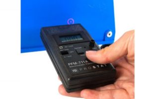
In order to establish a meaningful FEOL electrostatic control program, initial and recurring audits are essential. The ANSI/ESD S20.20-2014 standard suggests, “If the field measured on the process required insulator is greater than 2000 volts/inch and the process required insulator is less than 30 cm (12 inches) from the ESDS item, steps shall be taken” to move or ionize the object.
This is intended to avoid ESD between product and nearby surfaces. While this is a good rule to follow for BEOL product protection, it is inadequate to minimize static-charge-enhanced micro-contamination in FEOL. In processes with sub-20 nm feature sizes, 10 nm particles can kill a die. The electrostatic forces on such small particles will overwhelm the intended cleansing action of Ultra Low Particle Adder filtered unidirectional air flow in a process tool.
For more information visit: http://www.cemag.us/article/2017/02/semiconductor-fab-electrostatic-charge-program-improvement-opportunities-and-pitfalls


