

Issues
To increase distance and capacity, it will be necessary to expand the frequency bandwidth that can be amplified while simultaneously supporting modulation methods that can transmit more information within the same frequency bandwidth, and a strong requirement is to have less distortion when the signal is amplified. Another pursuit is keeping in check the energy consumption of communication systems that accompanies greater distances and capacities, and the improved energy efficiency in power amplifiers.
About the Newly Developed Technology
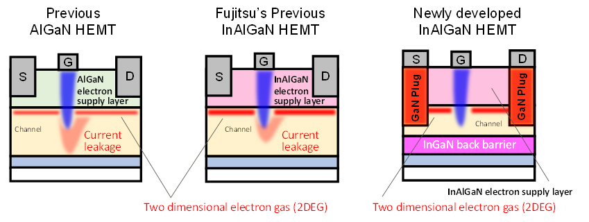
In order to both increase the distance and capacity of wireless communications and decrease energy consumption with indium-aluminum-gallium-nitride (InAlGaN) HEMTs, Fujitsu has developed two technologies that effectively reduce internal resistance and current leakage. Features of the newly developed technologies are as follows:
1. Technology to reduce internal resistance
Fujitsu has developed device technology that can reliably reduce resistance to one tenth that of previous technology when current flows between the source or drain electrodes and the GaN-HEMT device. The technology utilizes a manufacturing process that embeds GaN plugs directly below the source and drain electrodes, which generate electrons at high densities (fig. 1).
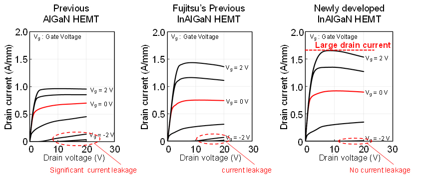
It is necessary to transport the electrons that come from the source electrode to the two dimensional electron gas field as smoothly as possible. The structure of the previous technology causes the electron supply layer to become a barrier, however, and internal resistance increases between the source electrode and the two dimensional electron gas. By applying this new technology, Fujitsu succeeded in running high currents through the transistor with significantly less resistance (fig. 2).
2. Technology to control current leakage
A current leakage occurs when the two dimensional electron gas, which moves at high speed on the boundary at the top of the channel layer, takes a detour below the gate when the transistor is in its off-state. This leakage causes deterioration in the operational performance of the power amplifier. Normally, it is possible to reduce current leakage by placing a barrier layer beneath the channel layer, but in that case the amount of two dimensional electron gas also decreases, and leads to a reduction of the drain current.
This new technology maintains high drain currents by effectively distributing indium-gallium-nitride (InGaN) to create a barrier layer below the channel layer. This reduces electron detours during operation, successfully providing significant reductions in current leakage (fig.1, fig. 2).
Effects
The previous world record for power amplifier output density in the W-band for transmitters was 3.6 watts per millimeter of gate width with technology developed by Fujitsu Laboratories. This has improved significantly with the newly developed technology, which delivers power output of 4.5 watts per millimeter of gate width for a power amplifier designed to operate at 94GHz. In addition, this new technology achieved a reduction in energy consumption of 26% compared to the previous technology through a reduction in current leakage. It is anticipated that the use of this power amplifier will allow the achievement of high capacity, long distance wireless communications between two connected systems at different locations at over 10Gbit/s and at distances greater than 10km.
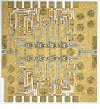 Figure 3: Picture of the newly developed W-band GaN-HEMT power amplifier chip
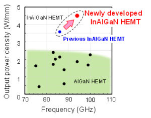 Figure 4: Comparison of GaN-HEMT power amplifier performance
Future Plans
Fujitsu aims to apply this technology broadly to the development of power amplifiers for purposes that call for wireless communications that offer long range and higher capacity, while offering easier installation than fiber optics. The goal is to commercialize this technology in high speed wireless communication systems by 2020, with an aim to employ it in such situations as a method of restoring communications when fiber optic cables have been severed by natural disasters or as a way of setting up temporary communications infrastructure when holding events.


