After a quiet period due to the saturation of the mobile handset industry, the GaAs wafer market wakes up. Apple, with its iPhoneX put under the spotlight on GaAs-based VCSELs , using for 3D sensing function. The technical choice made by Apple creates a real and vast enthusiasm for GaAs solutions. 3D sensing in mobile phone as well as LiDAR’s applications are so giving a new breath for GaAs substrates suppliers.
As one of the most mature compound semiconductors, GaAs has been ubiquitous as the building block of power amplifiers in every mobile handset. In 2018, GaAs RF business represents more than 50% of the GaAs wafer market. However, market growth has slowed down in the past couple years due to the handset market’s gradual saturation and shrinking die size. “At Yole, we expect GaAs to remain the mainstream technology for sub-6 GHz instead of CMOS, owing to GaAs’ high power and linearity performance as required by carrier aggregation and MIMO technology,” explains Dr. Hong Ling, Technology and Market Analyst at Yole.
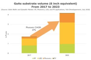
Since 2017, GaAs wafer has been particularly notable in photonics applications. When Apple introduced its new iPhone X with a 3D sensing function using GaAs-based lasers, it paved the way for a significant boost in the GaAs photonics market. GaAs wafers market segment for photonics applications should reach US$150 million by 2023.
“GaAs-based ROY and infrared LED applications have also caught our attention”, asserts Dr. Ezgi Dogmus, Technology & Market Analyst at Yole. “We estimate, 2017-2023 CAGR achieves 21% (in units) for the total GaAs LED market, surpassing more than half of GaAs wafer volume by 2023.”
 ““At Yole, we expect GaAs to remain the mainstream technology for sub-6 GHz…”
(Dr. Hong Lin, Technology & Market Analyst, at Yole)
In terms of the wafer and epiwafer businesses, each application requires a different size and quality when determining wafer and epiwafer prices. As a new entrant, photonics applications will impose new specification requirements compared to the well-established RF and LED wafer and epiwafers, creating significant ASP diversity.
From a value chain point of view, the GaAs photonics market’s remarkable growth potential will offer plenty of opportunities for wafer, epiwafer, and MOCVD equipment suppliers, as well as for investors.
GaAs wafer supply: Sumitomo Electric, Freiberger Compound Materials, and AXT, involved in GaAs wafer supply, lead the market with about 95% of market share collectively. And since new laser applications have very high specification requirements for GaAs wafer that are constantly evolving, Yole analysts’ expect the top players to maintain their technical advantage for at least another 3 – 5 years.
Regarding GaAs epiwafer production, Yole’s analysts identified different business models. The GaAs LED market is principally vertically integrated, with very well-established IDMs like Osram, San’an, Epistar, and Changelight. In parallel, GaAs RF businesses outsource significantly from well-established epihouses.
Within the GaAs photonics market, the epi business is still applications-dependent. GaAs datacom market segment is mostly epi-integrated, with dominant IDMs like Finisar, Avago, and II-VI. For 3D sensing in smartphones, epi outsourcing is significant.
Under its new technology & market report “GaAs Wafer & Epiwafer Market: RF, Photonics, LED and PV applications”, Yole Développement (Yole) announces a 15% CAGR between 2017 and 2023 (in volume), with an impressive 37%, especially for photonics applications.


