What is a PCB?
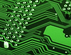
A Printed Circuit Board (PCB) is what connects all the electrical components inside an electronic device. It is a small green board made out of precious metals that are essential to the function of electronics. You will find a PCB in most electronic devices.
What Does a PCB Do?
The PCB inside electronics is what allows them to function as they are intended too. Without PCBs, electronics would not work. Through the conductive tracks, pads and other portions of the PCB, it helps connect all the electronic components within the intended device.
History of PCBs
There is a long history of a PCB. It goes back to 1943, developed by Australian scientist Dr. Paul Eisler. However, the development of PCBs goes back into the early 1900s when patents for what is known as “printed wire” were requested. It was an electrical path which was directly made onto an insulated surface. Many different scientists fiddled around with laminated conductors to an insulated board. In 1904 Thomas Edison used chemical methods to plate conductors to linen papers.
In 1925, US citizen Charles Ducas submitted a patent for creating an electrical path right on to an insulated surface. This was done through a printing a stencil with electrically conductive ink.
However, it was Eisler that created the first operational board to replace radio tube wiring. In 1936 he began work on a printed circuit for a radio set. In 1943 during World War II, the United States started to use technology to develop proximity fuses on a large scale.
Typically PCBs were made out of different materials, including Masonite and thin wooden planks. It wasn’t until the 1950s when other materials were used that they became common in household electronics. Before that, they were more intended for government usage.
As the years continued and PCB’s continued to evolve, new methods came to the front for developing the boards. Copper replaced the other materials involved in making the board because of it being an excellent way to carry electrical currents at a low cost. They also were required to be smaller in size as the demand for smaller electronics increased.
Manufacturing Process of PCBs
There are multiple steps included when manufacturing a PCB. To correctly assemble a PCB, the environment must be clean to keep all the components free from contamination. Here is an example of building a standard two-sided PCB:
“PCB Manufacturer in INDIA“
-
Start With the Design:
Using a PCB design software, the designer comes up with what the PCB will look like and how it will function. The designer should include information like the copper tracking layers, all components involved, drill drawing and anything else that contributes to the PCB. It is then sent for production.
-
Creating a Film:
The design of the PCB is then printed using a special machine (plotters) that creates photo films of the PCB. These machines are specially made for this process to achieve precise printing and high details. You then have a plastic sheet with ink resembling different layers of the PCB.
-
Printing the Inner Layers:
This step is when the physical creation of the PCB begins. The substrate level starts by using an epoxy resin mixed with a glass fibre (prepreg). Copper is then bonded to both sides and then whittled away to reveal the design of the board. A photosensitive film (resist) is then added to the panel.
-
Remove Excess Copper:
Any unwanted copper left on the board is then removed. A chemical solution eats the excess copper away. The hardened photoresist protects the wanted copper.
-
Aligning the Layers:
All the layers of the board need to be aligned and punched together. Holes on each layer are lined together and sent through an optical punch machine. From here on out, any errors found on the inner layers cannot be corrected.
-
Layer Together:
Here is when the PCB takes its shape. The additional layers are fused together with the substrate. They are then bonded together to ensure they fit securely together.
-
Drill:
Holes are then drilled to keep the layers from being plated.
-
Plating:
The PCB then goes into the plating process to fuse everything together. The board is immersed in copper, after being thoroughly cleaned, to create a thin plate.
-
Outer Layer Resist:
Once again, a photoresist layer is added to the out layers, and the board is ran under UV lights.
-
Second Plating:
There is another step of plating needed with a layer of copper. From the previous copper plating, a layer of tin is applied to prevent any of the wanted copper from being etched off.
-
Final Etching:
The same chemical solution again removes unwanted copper from the board. This establishes the proper conducting areas and required connections.
-
Solder Mask Application:
The cleaned board is covered with an epoxy solder mask and blasted with a UV light.
-
Finishing Touches:
The board is then plated with either gold or silver to add solder quality to it. Then the board goes through an ink-jet writing process onto the surface which holds critical information for the board. It is then coated and cured for the last time.
Read How Does a PCB Work & What are the Components of a PCB


