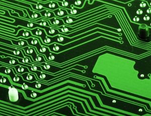
Fiberglass layers are stacked on top of each other and treated with a resin to keep them together. They are then covered with a copper layer on either side and then coated with a photoresist. It is then covered with the design that ultimately holds the controls of the board. They look like tracks on a PCB. Those tracks are the electrical connections that power the electrical device.
What is the Material Used in a PCB?
PCB’s tend to have a copper layer and an insulating layer that is laminated to the substrate. The substrate is typically made out of a fiberglass epoxy resin and bonded with copper foil. There is also the use of tin for layering the copper circuits to prevent oxidation. You will also find materials like gold, silver, nickel, aluminum and palladium during certain aspects of the PCB development.
What are the Components of a PCB?
Each component is vital to the overall board. They all have their own task for the PCB to function correctly. Typically you would find the following elements on a standard Printed Circuit Board:
- Battery – provides the voltage to the board.
- Inductor – stops and changes in the current.
- Diode – what makes the current flow in one direction.
- Switches – depending on if they are opened or closed, they will block or allow current.
- Resistors – they are color coded to determine how much current passes through.
- LEDs – (light emitting diode) lights that illuminate when current is flowing and allows only enables the flow of one current in one direction.
- Capacitors – holds an electrical charge.
What is a PCB Layout Software?
A PCB Layout Software is what is used during the initial design step of developing the board. The software is what generates the design of the board which is then taken into the production steps. Depending on the type of board you are developing, and what the intent is, that will determine which software you use.
What is the Use of a Printed Circuit Board?
A PCB is used for electronic devices, no matter the size. The small board not only powers the components in the device, but it also powers the whole device itself. Without the PCB the electronic machine would not function to its full intention.
A PCB also makes the development process of electronics a little more simplified. Before the invention of a PCB, the inside of an electronic device would be scrambled with wires and connections. This meant the device needed to be fairly large to hold all of the wires. Now a PCB simplifies the connection which allows for devices to be much smaller in size.
PCB Terminology
There is a lot of different terminologies used to describe what a Printed Circuit Board is. Here are some of those terms:
- Pad – the exposed metal on the surface of the board which has a component soldered to.
- Substrate – this is a physical structure that holds the components.
- Single-Sided – all the components are on one side of the substrate.
- Double-Sided PCBs – when there are too many components for a single-sided PCB, a double-sided board is used.
- Multi-Layered – the substrate is separated by layers of insulation with components connected through plated holes.
- Flexible PCBs – boards made with flexible materials when special constraints limit the use of a rigid circuit board.
- Buried Vias – the vias make the connection between the layers of a PCB. Buried vias connect multiple inner layers without going through the outer layer.
- Thick Printed PCB – the thickness level of the board influences the functionality of the board.


