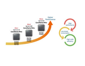
Renesas Electronics Corporation (TSE:6723), a premier supplier of advanced semiconductor solutions, today announced the development of its third-generation 32-bit RX CPU core, the RXv3. The RXv3 CPU core will be employed in Renesas’ new RX microcontroller (MCU) families that begin rolling out at the end of 2018. The new MCUs are designed to address the real-time performance and enhanced stability required by motor control and industrial applications in next-generation smart factory, smart home and smart infrastructure equipment.
The innovative RXv3 core boosts the proven Renesas RX CPU core architecture with up to 5.8 CoreMark/MHz, as measured by EEMBC® Benchmarks, to deliver industry-leading performance (Note), power efficiency, and responsiveness. The RXv3 core is backwards compatible with the RXv2 and RXv1 CPU cores in Renesas’ current 32-bit RX MCU families. Binary compatibility using the same CPU core instruction sets ensures that applications are written for the previous-generation RXv2 and RXv1 cores carry forward to the RXv3-based MCUs. Designers working with RXv3-based MCUs can also take advantage of the robust Renesas RX development ecosystem to develop their embedded systems.
“The cutting-edge RXv3 core technology targets a wide range of embedded applications in the industrial IoT era where ever-increasing system complexity places higher demands on performance and power efficiency,” said Daryl Khoo, Vice President Product Marketing, IoT Platform Business Division, Renesas Electronics Corporation. “The EEMBC CoreMark/MHz processor benchmark clearly shows the RXv3 core outperforms all competing CPU cores. Once again, Renesas delivers superior MCU performance and power efficiency to our customers’ next-generation embedded systems.”
Key Features of the RXv3 CPU Core
The unique RX CPU core combines a design optimized for power efficiency and a fabrication process producing excellent performance. The new RXv3 CPU core is primarily a CISC (Complex Instruction Set Computer) architecture that offers significant advantages over the RISC (Reduced Instruction Set Computer) architecture in terms of code density. RXv3 utilizes a pipeline to deliver high instructions per cycle (IPC) performance comparable to RISC. The new RXv3 core builds on the proven RXv2 architecture with an enhanced pipeline, options for register bank save functions and double precision floating-point unit (FPU) capabilities for the highest computing performance, power and code efficiency.
Superior Computing Performance and Power Efficiency
- Enhanced RX core five-stage superscalar architecture enables the pipeline to execute more instructions simultaneously while maintaining excellent power efficiency
- The RXv3 core will enable the first new RX600 MCUs to achieve 44.8 CoreMark/mA with an energy-saving cache design that reduces both access time and power consumption during on-chip flash memory reads, such as instruction fetch
Fastest Response Times
- The RXv3 core achieves significantly faster interrupt response times with a new option for single-cycle register saves
- Using dedicated instruction and a save register bank with up to 256 banks, designers can minimize the interrupt handling overhead required for embedded systems operating in real-time applications such as motor control
- RTOS context switch time is up to 20 percent faster with the register bank save function
Unrivaled Double Precision FPU Capabilities
- The model-based development (MBD) approach has penetrated various application developments; it enables the DP-FPU to help reduce the effort of porting high precision control models to the MCU
- Similar to the RXv2 core, the RXv3 core performs DSP/FPU operations and memory accesses simultaneously to substantially boost signal processing capabilities


