


2.5D and 3D stacking technologies are the only solution that meet the required performance of applications like AI and datacenter as for today”, confirms Mario Ibrahim, Technology & Market Analyst from Yole Développement (Yole). Stacking technologies are used in a variety of hardware, including 3D stacked memory, GPU , FPGA , and CIS , are intended for the high/mid and low-end market segments.
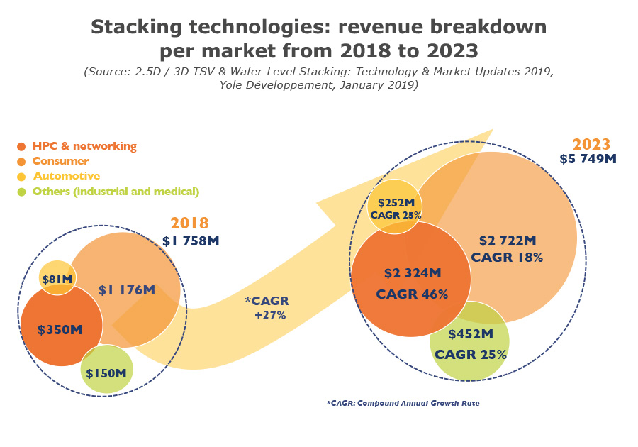
Hardware like HBM and CIS comprise the majority of TSV’s revenue. The overall stacking technologies market will exceed US$5.5 billion in 2023 with a CAGR of 27%, announces Yole it its latest advanced packaging report, 2.5D / 3D TSV & Wafer Level Stacking: Technology & Market Updates report. As for today, the consumer market is the biggest contributor, with over 65% market share. But this, paradoxically, doesn’t mean that consumer is the driver for these technologies. In reality, HPC is the real driver for stacking technologies and will exhibit the fastest growth up to 2023, with market share doubling from 20% in 2018 to 40% in 2023. In terms of packaging revenue, this equates to a more than 6x increase from 2018’s revenue. Consequently, the consumer market’s share will decrease. Other markets like automotive, medical, and industrial will maintain their current market share.
For today’s high-end market segment, the most popular 2.5D and 3D integration technologies on the market are based on TSV for 3D stacked memory, and TSV interposer for heterogeneous stacking. CoWos technology is already widely used for HPC applications, and new TSV technologies will hit the market in 2019. As an example, Foveros from Intel is based on “active” TSV interposer and 3D SoC technology, with hybrid bonding and TSV interconnections (potentially). Foveros from Intel shows, although TSV is being challenged by non-TSV technologies, companies still have faith in it.
In parallel, Yole’s analysts also underline the emergence of TSV-less technologies in the market. Such innovations can be placed into two groups: “with substrate” and “embedded in substrate”.
EMIB technology, already commercialized, is part of the embedded-insubstrate group, where the silicon bridge is deep seating in the substrate. Within System Plus Consulting EMIB report, Stéphane Elisabeth, Expert, Cost Analyst at System Plus Consulting underlines Intel’s expertise: “In the past few years, needs for high DRAM bandwidth has led to increasing investments to develop innovative packages. Localized high density interconnects devices between two or more dies has so been investigated. Objective was clearly to provide a higher bandwidth signal in order to open up new opportunities for heterogeneous on-package integration.”…Typical proposed devices are today glass, organic or silicon interposers. And Intel has developed its own approach with EMIB solution, which offers simpler integration.
With-substrate technologies are also used as alternatives to TSV. For example InFO on substrate is widely used in Apple’s processors. Also, RDL interposer technology is currently being developed and will hit the market by 2020. Last but not least, FOCoS was developed and commercialized in 2016, but seems to be lacking orders.
Hybrid bonding can bridge the two main categories (with TSV/without TSV). This technology’s particularity is that it can be simultaneously TSV challenger and teammate. Since 2016 it has been commonly used in smartphones’ CIS, and in the near future it will integrate the high-end market segment for memory and 2.5D as an interconnection solution…


