Enhanced technology can monitor a vessel’s full surroundings day or night up to six nautical miles away, automatically differentiating objects in concert with Deep Learning AI technology
Fujitsu Limited and Fujitsu Laboratories Ltd. today announced the development of a miniaturized photodetector for high-sensitivity infrared cameras. In the future this breakthrough sensor technology will allow for infrared cameras just one eighth the size of previous models able to take detailed images even at night or at a distance.
There are considerable expectations surrounding the use of high-sensitivity infrared cameras in the navigation of ships under human observation. These cameras are capable of taking high resolution images from a distance of up to six nautical miles (about 11 kilometers) during day or night. The photodetectors in these cameras remain susceptible to thermal noise, however, and since the equipment required for cooling them is quite large, it became necessary to find a way to reduce the cameras to a practical size.
With the development of a sensor semiconductor structure that reduces the impact of thermal noise, Fujitsu Laboratories has made it possible to create handheld-sized, high-sensitivity infrared cameras. In addition to this breakthrough, Fujitsu Limited has applied AI technology to process the images taken with the infrared cameras, and succeeded in automatically identifying ships cruising up to six nautical miles away.
With miniaturized, high-sensitivity infrared cameras installed around the circumference of a ship, this enhanced technology will allow for the identification of distant vessels without false positives. In so doing, Fujitsu will help realize the development of autonomous cruising technology and promote safer navigation for ships.
Development Background
The demand for safer navigation technologies has grown along with the increase in marine shipping volumes accompanying the growth of international trade in recent years, as well as heightened anticipation around the advent of autonomous ship navigation.
When cruising, it remains critical for navigators to accurately grasp the location of obstacles in the area, such as other ships and buoys, in order to avoid accidents. For this reason, it is usually necessary to understand a ship’s surroundings up to about six nautical miles out (about 11 km).
Issues
When looking for cameras capable of taking highly detailed images, even at night or at a distance, attention has focused on high-sensitivity infrared cameras, which are capable of capturing images at about twice the distance of ordinary infrared cameras. High-sensitivity infrared cameras, however, absorb infrared light through photodetectors susceptible to thermal noise, making it necessary to maintain an extremely low operating temperature of about 95K (about -178°C). The need for powerful cooling equipment for the photodetector has resulted in making the cameras relatively large, which renders them unsuitable for use in applications that require the installation of multiple cameras for full-surround monitoring, including aboard ships.
Consequently, in order to improve the safety of navigation and monitor the surroundings of a ship underway without blind spots, it proved necessary to reduce the size of the cameras as a whole. For this reason, increasing the operating temperature of the photodetectors and reducing the burden of cooling equipment represented a significant issue.

About the Newly Developed Technology
Fujitsu Laboratories has now developed a semiconductor structure that can raise the operating temperature of the photodetector without reducing its sensitivity compared to existing high-sensitivity infrared cameras.
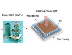
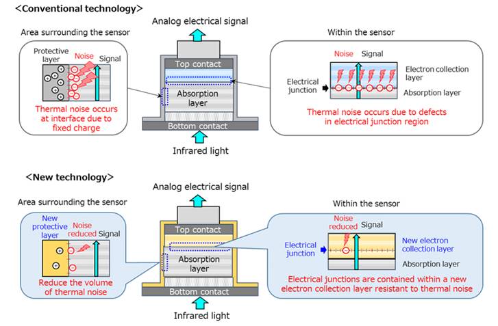
The photodetectors of high-sensitivity infrared cameras directly convert the absorption of infrared light into electrical signals. During this conversion, the energy absorbed from the infrared light, as well as extraneous electrons are excited by heat energy, creating unwanted electrical signals (thermal noise).
Thermal noise consists of two components: this includes the noise that occurs around the edges of the sensor, specifically at the interface between the sensor and the protective layer that covers its edges, and noise that occurs within the sensor itself. This newly developed technology reduces defects in the interface with the protective layer, which is formed at low temperatures. Meanwhile, the electric charge contained in the protective layer is controlled to avoid unwanted charge from the interface, thereby limiting the thermal noise from the surroundings caused by defects and charge concentration.
Moreover, Fujitsu Laboratories has strengthened the resistance against thermal noise of the electron collection layer that connects to the absorption layer, which consists of alternate layers of semiconducting thin films of indium arsenide (InAs) and gallium antimonide (GaSb). The electrical junction region that is the source of thermal noise within this component has also been shifted from the contact surface between the electron collection layer and absorption layer and toward the strengthened electron collection layer, effectively reducing the volume of thermal noise within the sensor.
With these two technologies, Fujitsu was able to raise the practical operating temperature of the photodetector by more than 50°C over previous technology, to 145K (about -128°C), making it possible to reduce the overall size of the camera, including the cooling component, to about one eighth its previous size.
Effects
By deploying multiple miniaturized high-sensitivity cameras, it has become possible for a ship to accurately detect other ships and small obstacles that could impede navigation up to a distance of six nautical miles without any blind spots at day or night. In addition, when AI technology (deep learning algorithms) was applied to images taken with this newly developed camera in an experiment to detect distant vessels, both false positives and false negatives were extremely low, and Fujitsu confirmed high differentiation performance (a differentiation rate of more or less 100% at 2-3 nautical miles distance).
This makes it possible to create a system for automatically monitoring surroundings from miniaturized, high-sensitivity infrared cameras and highly detailed images, which are anticipated to prove useful in avoiding accidents at sea and for autonomous navigation.

Future Plans
Fujitsu Laboratories and Fujitsu Limited aim to commercialize this technology as a service in 2020, after confirming the effectiveness of a monitoring system that incorporates the new technology through field trials, including monitoring the areas surrounding a ship. The companies will additionally consider the application of this technology to autonomous navigation, with the goal of bringing about safer and more secure maritime navigation.


