


In a new study released during the February 2019 Mobile World Congress in Barcelona, by mobile communications industry researchers, GSMA, it was projected that 5G networks will account for 15% of all global mobile connectivity by 2025. A number of new industry-wide 5G compatible device launches are set to begin as soon as April 2019. Overall 5G network performance goals center around improved device connectivity, higher-speed data rates, reduced latency, energy and cost savings, and expanded system capacities.
The needs for such higher speeds and increased system capacities can be attributed, in part, to the equally sharp, observable increases in Internet end-user traffic volumes, as well as cellular phone and mobile device usage. Those needs have led to an emerging demand for communication systems that are capable of required ultra-high-speed, large-capacity signal processing. In the case of wired systems, such as optical fibers, advances in time division multiplexing (TOM) and wavelength division multiplexing (WOM) systems can offer such enhanced signal-handling capacities. For wireless systems, such as cellular phones, the use of higher frequency bandwidth is essential to device performance reliability. In the case of wired systems, such as optical fibers, TOM –which implements time-based multiplexing in circuitry—can offer certain advantages over WOM. For example, TOM allows for simplified system construction, more compact communication systems, and lower overall system costs. The favorable characteristics of TOM have further increased industry demand for development of ultra-high-speed electronic devices with TOM compatibility.
While GaAs and SiGe semiconductor components are typically specified for commercial transfer speeds of up to 10 Gbits/s, many observers believe that the performance ceilings of these materials will limit maximum transfer rates to slightly at or above 40 Gbits/s. For ultra-high-speed circuits of the over-40-Gbit/s class, as well as ultra-high-speed analog-and-digital mixed circuits, anticipation is currently running high for devices whose designs incorporate faster lnP semiconductor components. Those components must be capable of meeting industry demands for increased performance speeds yet must not sacrifice operating margins for device manufacturers.
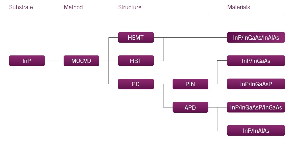
Among the several types of lnP electronic devices, research and development is currently active in the commercialization of both heterojunction bipolar (HBT) and high-electron mobility transistors (HEMT). Since lnP semiconductors offer higher average carrier throughput than can be found with ordinary saturation velocity, they present significant advantages in these applications. One such advantage is their favorable current gain cut-off frequency (fT), an important transistor performance parameter.
Determinations of the basic performance characteristics of related transistor elements, such as lnP HBT and HEMT, is largely dependent on the material and structural properties of the chipset epitaxial layer itself. From a technology standpoint, the creation of a stable supply of low-cost chipsets with uniform element characteristics and circuitry properties requires elevated uniformity in both epitaxial layer composition and film thickness, combined with reduced impurity content rates. Further design goals include improvements in heterojunction interface quality, as well as growth techniques for ensuring reproducibility. The successful development of mass-production technologies for achieving these goals is the topic of recent research undertaken by the Latham, New York-based Marktech Optoelectronics, Inc., as described herein.
The R&D approach was carried out in two unique phases. The first phase consisted of the development of ultra-high-speed lnP epitaxial crystal growth technology using small prototype MOCVD equipment (4inch.x4). The second phase consisted of the development of ultra-high-speed lnP epitaxial crystal manufacturing technologies using large mass-production MOCVD equipment, known as GAKOUS (4inch.x10). The small MOCVD prototype created from this effort was observed to exhibit favorable performance characteristics with respect to new organic metal materials via an independent source injection. A narrow gap between the injector and surface was placed to mitigate the risk of complex surface reactions. From an evaluation of the prototype, Marktech was able to conclude that it had successfully developed a series of new manufacturing equipment, MOCVD GAKOUS, whose production capabilities offered the same uniformity as the prototype.
The second R&D phase was the Marktech development of lnP HBT epitaxial crystal growth technology which could successfully achieve the required ultra-high-speed large-capacity signal processing capabilities. As a first step, Marktech recognized the favorable influence on HBT device electrical performance characteristics which could be achieved by a new manufacturing method: carbon-doped InGaAs growth without hydrogen.
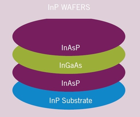
Techniques for Marktech InP HBT epitaxial crystal growth development first incorporated hydrogen-carbon doped lnGaAs, then measured basic prototype optical characteristics and hydrogen concentration data. The team then tried to use new organic metal materials, in combination with Triethyl Indium (TEI), Triethyl Gallium (TEG), Triethyl Arsen (TEAs) and Carbon tetrabromide CBr4 for carbon-doped lnGaAs. It then compared conventional data for Trimethyl Indium (TMI), TEG, Arsine (AsH3) and CBr4. Marktech then experimented with several conditions for making carbon-doped lnGaAs using the new prototype MOCVD system with TEl, TEG, TEAs and CBr4. From those efforts, the team was able to produce an lnGaAs wafer prototype which offered a carrier concentration over 5E19cm-3 as a grown condition. Desired uniformities in thickness and a doping concentration of less than 2% were achieved with four-inch wafers. Marktech also achieved the necessary prototype growth technology reproducibility that is essential to manufacturing production quality control. As true lnP-HBT epitaxial crystal performance testing requires an evaluation of electrical characteristics on larger HBT devices, it is difficult to estimate actual HBT device performance. Instead, Marktech focused development efforts on new manufacturing technologies, capable of the rapid uniform production of smaller-sized InP-HBT epitaxial crystals with good reproducible quality. The team further performed successful high-frequency HBT electrical characterizations on the smaller prototype.
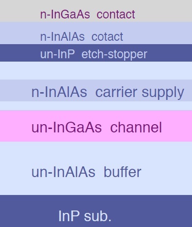
In its further development of lnP HEMT epitaxial crystal growth technologies, Marktech confirmed that it was possible to achieve both the desired film thickness and sheet resistance within the appropriate ±2% InGaAs distribution for a 4-inch wafer, with lnAIAs single-layer epitaxial crystals. These desired characteristics could be further achieved using the same MOCVD small prototype equipment created during phase 1 development. Marktech first promoted the growth of an lnP HEMT crystal structure, in order to assess basic device electrical performance characteristics. The team then analyzed material dependency based on channel layer quality. From that effort, using TEI, Marktech developed a 10% higher electron mobility in the lnGaAs channel layer. As the cracking temperature of TEI is lower than that of conventional TMI materials, lnGaAs crystal quality is thereby improved, as the carbon concentration is low. In addition, electron mobility depends on the Indium concentration of the lnGaAs channel layers. Normal lattice matched structure is InxGaAs:Inx=0.53. Marktech further developed a high-indium concentration channel layer (lnxGaAs: lnx=0.7) without any lattice distortion.
In general, the achievement of good lnP channel layer quality requires higher growth temperatures and generous PH3 flows. However, the relatively higher material costs of PH3 posed a challenge during the mass production phase. To address this concern, Marktech developed lower growth temperatures and lower-cost PH3 technologies, via the use of Triethyle phosphorus (TEP). In doing so, the team successfully achieved a 1/10 maximum reduction in PH3 flow rate expenditures, with reduced costs, without sacrificing quality.
As a final accompaniment to this research, Marktech focused efforts on the development and introduction of non-destructive electron mobility measurement systems. As it is possible to estimate channel layer carrier concentrations with HEMT, channel layer thicknesses could be evaluated via X-ray diffraction pattern analysis and spectroscopic ellipsometry. Marktech also developed testing techniques for time-resolve photoluminescence with infrared wavelength area measurements. These were proven useful in the performance of lnGaAs channel layer quality checks, as well as HBT gain estimates by p-lnGaAs base layers.

The small MOCVD prototype 4inchx4 exhibited satisfactory performance with new organic materials, independent source injection and a narrow gap placed between the injector and surface to avoid complex surface reactions. As a result, Marktech developed its original manufacturing type MOCVD GAKOUS equipment to achieve the same performance as that of a 4inchx10, with sufficient quality and uniformity for lnP HBT and HEMT mass production.


