


RIBER is announcing that an operational licensing agreement has been signed with Toulouse Tech Transfer (TTT) for the exclusive marketing of a reflective surface defect and curvature measurement technology, developed by the LAAS-CNRS.
Dedicated high-precision metrology technology for semiconductors manufacturing
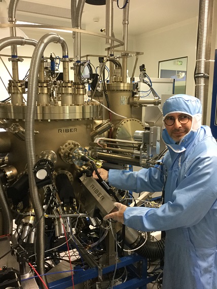
The LAAS-CNRS researchers Alexandre Arnoult, research engineer, and Jonathan Colin, post-doctoral researcher, have developed a sophisticated optical device that is easy to implement and helps to significantly improve control over operations to deposit thin films. The device can be used in any type of environment.
This makes possible to measure curvature and defects on all types of surfaces in real time and over significant production times. For example, it helps to avoid dislocations, produce perfectly even wafers or control deposit consistency. The device will also be equipped with machine learning algorithms that will be specially developed to optimize analysis and control for the materials growth process.
EZ-Curve: new technological component for RIBER’s strategic development
Capitalizing on all technology the know-how based on this research, marketed under the new EZ-Curve brand will enable RIBER to extend its range of solutions and services, providing research laboratories and semiconductor manufacturers with added value in line with their needs.
For industrial users, ensuring the traceability and reliability of their measurements is key to effectively manage their manufacturing processes and guarantee products quality and performance. For researchers, analyzing and understanding materials growth-related behaviors makes it possible to expand fundamental knowledge.
The EZ-Curve solution is a major innovation on the molecular beam epitaxy (MBE) market. In addition to controlling the epitaxial growth process with high-precision 3D reflectance metrics, this device also offers wider possibilities by supporting the implementation of automated advanced control processes and, over the longer term, the development of smart MBE systems.
Philippe Ley, RIBER’s CEO: “EZ-Curve is a significant technological innovation compared with the measurement instruments currently available on the market. Our ambition is to provide our clients with the very precise levers needed to considerably improve their processes and the results of their developments, whether they are academic or industrial. This new technological component and its industrialization will make it possible to further strengthen MBE performance capabilities”.
This new device offers a range of benefits: non-invasive, cost-effective, portable, lightweight, easy to install and use, EZ-Curve is perfectly adapted for in-situ epitaxial process analysis.
“Monitoring a wafer’s deformations during the vacuum growth or processing of a thin film represents an unrivalled source of information on the atomistic processes involved, and quality control for industrial processes. Until now, this monitoring was reserved for specialists using tools that were complex to master. Our new technology successfully makes it possible to achieve this combination of increased sensitivity with outstanding robustness and simple implementation, which enables to deploy it across a large number of advanced and/or production systems. For example, we can now continuously monitor molecular beam epitaxy growth for complex semiconductor structures with low constraints, opening up possibilities for in-situ feedback control during processes, and therefore optimization and automation of processes”, confirms Alexandre Arnoult – LAAS-CNRS.
Following maturation and market release phases, RIBER, the LAAS-CNRS and TTT intend to continue sharing their knowledge in order to support this product’s development worldwide.
TTT’s 100th transfer
The technology transfer by TTT’s teams has focused on creating value and industrializing the EZ-Curve solution in order to facilitate its integration and its marketing by RIBER. This 100th license set up by TTT is a major milestone in its development since it was created in 2012. It illustrates the numerous actions carried out to create value through and capitalize on French public research to support national competitiveness.
Pierre Dufresne, CEO of Toulouse Tech Transfer, is delighted with this 100th license: “This is the result of the collaboration between teams from RIBER, the LAAS-CNRS and TTT. They have worked on this transfer with enthusiasm and pragmatism. Throughout the project, the teams have remained available and successfully worked with confidence to achieve their goals. TTT is proud to have been able to contribute to this technology’s maturation so that RIBER can rapidly bring its innovative product to the market”.
Understanding, controlling and automating thin-film deposition
The production of semiconductor alloys involves vacuum deposition of thin films of materials on an optically reflective wafer. The growth of this structure in vacuum, which may be as thin as just a few atomic layers, can involve mechanical constraints and deformations, which can be measured and controlled in order to make the process more efficient.
Today, several techniques enable to monitor deposition deformations in real time and with a non-invasive approach. However, these less precise systems are generally complex to implement, expensive and can only be used in certain specific experimental conditions.
The device developed by the LAAS-CNRS, comprising optical elements and interfaced with CrystalXE (software solution developed by RIBER to continuously adjust the deposition process with unrivalled levels of precision), delivers a range of undeniable benefits for MBE performance.


