


When it comes to portable devices, power adapters have, for some time, been the elephant in the room. Their size, efficiency levels and lack of power output have somewhat undermined the relentless decrease in the form factor of the devices they are supporting and therefore detract from their portability.
Now, USB power delivery (PD) offers the ability to deliver up to 100 W of power alongside data over a single cable. This convenience means that USB PD is becoming the preferred charging approach for small and medium devices. However, a challenge in implementing USB PD, is to deliver varying output voltages at higher power levels for the much-sought rapid charging, while not ending up with an adapter that is inefficient, costly and cumbersome.
Using wide-bandgap semiconductors, such as GaN power devices, is one potential approach to improve adapter efficiency and shrink adapter size, but this is an emerging technology in the field, and, at the moment, relatively expensive route to take. As an alternative, advances in topologies, such as active clamp flyback, use standard super junction MOSFETs that allow designers to fall back on proven technology, while still advancing adapter design.
We live in an increasingly mobile world where we carry multiple devices such as smartphones, laptops and tablets with us – as well as an increasing array of wearable devices for health monitoring and other applications. Manufacturers have invested huge sums of money in research and development to meet consumer demands including increased functionality and reduced size / greater portability.
When we travel, we begin to realize that while manufacturers have made huge progress in the miniaturization of the devices themselves, the necessary power adapter / charger has lagged behind somewhat and can be bulky in comparison with the device. This is especially apparent when traveling where multiple chargers are often required to suit the voltage and connector requirements of differing devices.
Clearly, some form of standardization is required to bring commonality to charging thereby reducing the number of chargers that must be carried, as well as reducing the electronic waste that is created by the huge number of chargers discarded every year.
USB 1.1 mandated power delivery of 2.5 W (5V, 500 mA) and USB 3.0 increased it to 4.5 W (5V, 900 mA), however this power capability was only suitable for small devices, such as smartphones. Released in 2012 by the USB Promoters Group, the USB PD specification allows for power transfers up to 100 W thereby allowing for larger devices, such as laptops and monitors, to be powered and mobile devices to be charged more rapidly. The ability to vary the output voltage also added to its versatility. There are a number of sophisticated features built-in to the standard including bidirectional power (allowing the device at either end of the cable to provide the power) and fast role swap which permits the delivery of data and power over the same cable at the same time.
When USB PD was first released it was based upon six power profiles that defined the voltage and current that could be delivered. However, USB PD 2.0 removed the profiles and allowed for a more flexible approach whereby power supplies can support any requirement from 0.5 W to 100 W.
While the flexibility delivered by USB PD may reduce the number of chargers required, it does not necessarily reduce the size of the individual charger and therein lays the challenge for designers. Not only must power adapters be compliant with USB PD, they must also increase their power density at a reasonable cost.
The path to achieving this is quite well trodden and power engineers intuitively know that increased efficiency is pivotal to achieving increased power density. More efficient designs generate less waste heat, meaning that the necessary dissipation can be achieved with smaller surface areas. In order to raise the efficiency, engineers look to highly efficient topologies and also improved components, especially key switching components. If these switching components have low dynamic losses, then switching frequencies can be raised, allowing bulky components such as magnetic devices to be reduced in size.
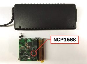
One area of focus at the moment are the wide bandgap devices such as gallium nitride (GaN) FETs that offer a number of benefits in terms of low losses, high temperature operation and fast switching frequencies. However, these devices remain relatively new and comparatively expensive. Additionally, they are somewhat unproven in long-term usage and, for this reason, engineers would prefer to rely on tried-and-tested silicon-based technology if comparable results can be achieved. One topology that is coming to the fore as a solution to the needs of modern power adapters is active clamp flyback (ACF). This uses variable frequencies to enable zero voltage switching (ZVS) of superjunction (SJ) FETs across multiple load and line conditions. This is implemented in the new NCP1568 AC-DC ACF pulse width modulation (PWM) IC from ON Semiconductor. Combining this new device with the new NCP51530 high performance 2 A 700 V half bridge driver provides engineers with a platform upon which to base future power adapter designs.
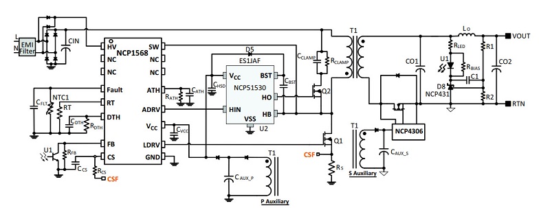
The NCP1568 acts as controller and provides the intelligence for the power system, allowing for ultra-high density and highly efficient power supply designs to be achieved. As well as ACF the controller operates in discontinuous conduction mode (DCM) enhancing efficiency in light load conditions while only consuming 30 mW of standby power, allowing designers to achieve compliance with modern efficiency specifications, including EU CoC Tier 2. The design is optimized for USB PD implementation, while requiring minimal external circuitry.
Operating at frequencies from 100 kHz to 1 MHz, allows designers to benefit from reduced size magnetics, thereby doubling power density compared to traditional flyback designs. With SJ FETs, the solution is able to achieve 93.5% peak efficiency and operates up to 400 kHz. The NCP1568 can also be used with eGaN FETs to push switching frequency and thus power density even higher.
While the NCP1568 provides the intelligence and control, the NCP51530 is an integrated high- and low-side driver that delivers efficient power switching of two N-channel power MOSFETs at voltage levels up to 700 V, thereby enabling high performance power solutions in compact spaces. The NCP51530 is well suited to high frequency operation with short propagation delays as well as fast rise and fall times. The tight matching of the propagation delays (5 ns) contributes to increased efficiency in all applications.
Summary
The USB PD specification goes a long way to addressing many of the challenges that have led to a plethora of different adapters being required for the many portable devices in use today. This streamlining will allow designers to re-focus efforts on making these adapters smaller and more efficient, preventing their size from negating the huge improvements that have been made in making portable devices even more portable.
While it is tempting to move to wide bandgap technologies such as GaN to address the power density challenge, this is considered by many to be risky in an area where reliability is crucial, mainly due to the fact that GaN remains relatively new and unproven.
The NCP1568 / NCP51530 pairing from ON Semiconductor meets the current needs of the market through a combination of a highly efficient topology (ACF) and high frequency operation that reduces component size. These benefits are achieved with reliable and proven silicon-based superjunction FETs although, the solution is also compatible with GaN devices once they achieve maturity.
The combination of high performance and proven technology is allowing many designers to remove the elephant from the room.


