


Leti, a technology research institute, has fabricated a fully integrated bio-inspired neural network. It combines resistive-RAM-based synapses and analog spiking neurons. The functionality of this proof-of-concept circuit was demonstrated thanks to handwritten digits classification.
The research work presented at IEDM 2019 measured a 5x reduction in energy use compared to an equivalent chip using formal coding. The neural network implementation is made such that synapses are placed close to neurons, which enables direct synaptic current integration.
“The entire network is integrated on-chip,” said Alexandre Valentian, lead author of the paper, “Fully Integrated Spiking Neural Network with Analog Neurons and RRAM Synapses”. “No part is emulated or replaced by an external circuit, as in some other projects. It even was used in a live demo where users could draw digits with their finger on a tablet and it is classified after conversion into a spike train.”
Spiking neural networks, also known as third-generation neural networks, are composed of bio-inspired neurons, which communicate by emitting spikes, discrete events that take place at a point in time, rather than continuous values. These networks promise to further reduce required computational power because they use less complex computing operations, e.g. additions instead of multiplications. They also inherently exploit sparsity of input events, since they are intrinsically event-based.
“To date, demonstrations of RRAM-based SNNs have been limited to system-level simulations calibrated on experimental data,” the IEDM paper explains. “In this paper, we present for the first time a complete integration of a SNN combining analog neurons and RRAM synapses.”
The paper explains that “the test chip, fabricated in 130nm CMOS, shows well-controlled integration of synaptic currents and no RRAM read-disturb issue during inference tasks (at least 750M spikes).”
“Data-centric workloads exhibited by Deep Neural Network (DNN) applications call for circuit architectures where data movement is reduced to a minimum,” the paper says. “This has motivated architectures in which memories are spatially located near the computing elements. These memories must be very dense, preferably non-volatile and inserted into the computational dataflow, therefore RRAMs are excellent candidates to this purpose.”
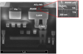
The study, which was supported by CEA-List, underscores CEA-Leti’s expertise at manufacturing RRAM memories on top of CMOS wafers.


