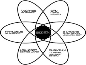
A collaboration between Nottingham-based start-up, SearchForThe Next (SFN) and Glenrothes-based Semefab introduced a new transistor architecture called Bizen (Bipolar/Zener). Bizen uses Zener quantum tunnel mechanics which promise to reduce production lead time, wafer area and process layers while increasing speed, reducing power and increasing gate density over CMOS.
Why Bizen….. Objective behind it
As Bizen requires only eight lithography masks, the new device can be produced just in three weeks’ lead time while CMOS process requires more masks and production takes around 15 weeks.
CMOS is facing the challenge of physical limitations of smaller and smaller structures. According to SFN, Bizen has potential to replace CMOS technology. Bizen offers 80 to 90% shorter cycle times, 3 times higher logic density, 60% better wafer surface area, high electromagnetic immunity, higher switching speeds and lower dynamic power consumption over CMOS.
Bizen (Bipolar/Zener)
Bizen is built upon the five decades old bipolar technology. David Summerland, CEO SFN explains: “The CMOS processing industry is hitting a brick wall as shrinking geometries bash up against the laws of physics. We went back to the very beginning and found a way to commercialize quantum tunnel mechanics in silicon or wide bandgap device manufacture. The result is ‘Bizen’ – Bipolar/Zener – which retains the advantages of traditional bipolar processing yet removes the disadvantages by using Zener quantum tunnel mechanics.”
Quantum zener effect tunneling has made it possible to obtain the advantages of the current-controlled bipolar technique while eliminating its disadvantages. Bipolar technology has traditionally been limited by its requirement for high-resistance resistors which have the disadvantage of occupying much space on the substrate. Bizen transistor allows designer to replace resistor with MOS device and take advantage of controllable current. This enables the realization of a very low power circuit in which the transistor is Normally-On but not saturated, and is controlled by an isolated tunnel connection, rather than a direct metal contact to the base well, as used in traditional bipolar transistors.
>Bizen uses Zener diode the reverse bias characteristic, which is produced by the abrupt change in doping levels between the n and p layers of the diode. This results in the generation of a quantum current.
Bizen Transistor
Bizen transistor has no direct metal connection to the base, which implies gate is isolated, the connection is formed by quantum tunneling.
Bizen transistor connections are named as anode 1 and 2 as there is no collector and emitter, it has the same characteristics in both current flow directions. The identical outputs (anode 1 and 2) are suitable for AC signals and push-pull circuits. The Transistors operate in normal-on but unsaturated and can be controlled via the tunnel junction – rather than by a direct metal contact to the base, as used in conventional bipolar transistors.
Bizen process can be used for digital transistors as well as power devices construction. For creating digital devices only four layers are required and available Switching voltage is in between 200 and 400mV ideal for high speed logic applications. Digital transistors can be created without any plasma metal edge.
Since mid-2017, SFN has been in collaboration with Semefab, the well-known, indigenous, privately-owned semiconductor and MEMS fab based in Glenrothes, Scotland, for process development and qualification leading to device production.
Semefab’s CEO, Allan James comments: ”If Bizen can be adopted by the industry, an important prize given the reduction in die area at a given technology node comparing a Bizen and CMOS logic implementation would be the ability to wind back the Moores’ Law clock by 10 years or more and bring many ‘previous-generation’ wafer fabs back into mainstream manufacture.” Though Bizen is not the only alternative for CMOS as researchers are working on technologies such as “Metal Air Gap” or MESO but they are still far from commercialization.


