What is Silicon Controlled Rectifier:
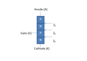
A Silicon Controlled Rectifier is a four layer, three terminal pnpn device with three junctions namely J1, J2, J3 with three terminals attached to the semiconductor materials namely anode (A), cathode (K) and gate (G). It has a large power handling capacity, high speed of operation, good trigger sensitivity, large power gain and long life with ease of maintenance.
SCR is one of the family member of thyristors which applies to a family of multilayer semiconductor devices that exhibit bistable (ON-OFF) switching action. It is made up of silicon material which converts high AC current into DC current (rectification) and controls high power and hence named as Silicon Controlled Rectifier.
The SCR is a rectifier since it has a forward direction in which it may have very low resistance and a reverse direction in which it has very high resistance. It is controlled since it can be switched from the high forward resistance (OFF) state to a low forward resistance (ON) state. Although the change in resistance is very large, it is brought by a very small value of control voltage or current.Structure of SCR:
Static Characteristics of SCR:
SCR has three basic modes of operation:
- Forward blocking mode (Off State): The SCR is said to be in forward blocking state when the anode is made positive with respect to the cathode junctions J1 and J3 are forward biased and junction J2 is reverse biased. The junction J2 will not allow the forward current to flow and only a small forward leakage current flows due to n1 and p2.
- Forward conduction mode (On State): SCR turns into conduction mode in two ways as either by increasing the forward voltage beyond the break overvoltage of the SCR or by applying a positive pulse to gate terminal. Once any of these methods are applied, the avalanche breakdown occurs at junction j2 and SCR turns into conduction mode.
- Reverse blocking mode: SCR is said to be reverse-biased when the cathode is made positive with respect to anode. Then junction J1 and J3 are reverse biased whereas J2 is forward biased. The device behaves in the same manner as two diodes connected in series with the reverse voltage applied across them. A small reverse current is produced as the reverse voltage is increased until the reverse avalanche region is reached. After this point, the reverse current increases rapidly as the reverse breakdown voltage.


