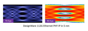
DesignWare IP With Unmatched Long-Reach Performance Results Supports Insertion Loss Greater Than 40dB & Delivers Power-Efficiency of Less Than five pJ/Bit
Synopsys announced the silicon proof of DesignWare 112G Ethernet PHY IP in 5nm FinFET process, delivering significant performance, power and area advantages. The area-efficient DesignWare 112G Ethernet PHY enables designers to optimize highly dense system-on-chips (SoCs) with placement-aware IP that maximizes bandwidth per die-edge through stacking and placement on all four edges of the die. To extend performance, the DesignWare 112G PHY demonstrates zero bit-error rate post forward-error correction in greater than 40dB channels while offering power-efficiency of less than five picojoules per bit (pJ/bit).
Combined with Synopsys’ routing feasibility study, packages substrate guidelines, signal and power integrity models, and thorough crosstalk analysis, Synopsys provides a comprehensive 112G Ethernet PHY solution for fast, reliable SoC integration. DesignWare 112G Ethernet PHY is an integral part of Synopsys’ comprehensive IP portfolio for high-performance cloud computing applications, including widely used protocols such as PCI Express, DDR, HBM, Die-to-Die, CXL and CCIX.
“As the industry’s trusted IP provider for over two decades, designers rely on Synopsys to deliver feature-rich, high-speed SerDes IP in the most advanced processes to help them gain a competitive advantage in the market,” said John Koeter, senior vice president of marketing and strategy for IP at Synopsys. “The comprehensive DesignWare 112G Ethernet PHY IP solution in 5nm FinFET process with differentiated performance, power and area enables designers to significantly reduce their integration risk for a faster path to silicon success.”


