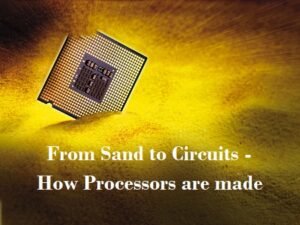
Have you ever imagined what is in the core of Silicon chips that power the world, how the sand we see in the environment plays an important part in building a circuit and what is in the heart of the electronic gadgets we use in our daily life? The answer to all these thoughts is hidden in the manufacturing of a processor which is an important part of Electronics and found in many modern electronic devices like smartphones, PCs, tablets, and other handheld devices we use in our daily lives.
In this article, we will discuss How Processors are made from Sand to give a complete Integrated Circuit used in this world of Technology, but before that let us read what a processor is.
What is a Processor?
A processor or “microprocessor,” is a small chip, an integrated electronic circuit, or a circuit board inside a computer that processes and responds to the basic instructions that drive a computer and other electronic devices.
The processor is considered as the brain of the computer that manages which operation is to be performed in a computer. It has two parts: Control Unit (CU) which manages the command and instructions to be performed and Arithmetic Logic Unit (ALU) which performs all the mathematical operations. The function of a Processor is to receive input in the form of program instructions and provide the output that the user will interface with by executing trillions of calculations.
How Processors are made?
Silicon is the starting or basic material for building a chip. It is a semiconductor material that can be turned into a conductor or insulator. Sand which is a result of the breakdown of Earth’s crust is made up of 25 percent silicon after oxygen. Quartz is a mineral present in the sand having high percentages of silicon in the form of Silicon Dioxide (SiO2) which is the base ingredient for manufacturing a semiconductor.
A journey of a processor from raw sand takes hundreds of steps and it is the most complex manufactured product in the world made in an ultra-clean environment. Below is a brief overview of this whole process starting from Sand to a Silicon chip and ultimately a complete Processor.
- Purification and Growing
The process begins when Silicon-rich sand is heated at a very high temperature and silicon is separated from the sand in the form of small tiny crystals. Before reaching a semiconductor manufacturing facility, the silicon is purified in multiple steps. The resulting purified electronic-grade silicon has one alien atom for every one billion silicon atoms. After purification silicon enters the melting phase and is made into a single solid cylinder-shaped continuous and unbroken crystal lattice, known as an ingot. - Mono-crystal Silicon Ingot
From electronic-grade silicon, mono-crystal silicon ingots are produced which weigh about 100 kilograms (roughly 220 pounds) and have a diameter of 300 mm with a silicon purity of 99.9999 %. - Slicing of Ingot
The ingot is cut and sliced thin into individual silicon discs called Wafers and their thickness is determined as per the requirement of a chip manufacturer. - Polishing of Wafer
After cutting, wafers are polished well to get flawless mirror-smooth surfaces. The polishing process goes on until all the roughness of the wafer surface turns into a smooth surface. These polished wafers are then sent to the chip manufacturing facilities for the fabrication process. - Photolithography
In this process, a specific pattern is imprinted on the wafer. While spinning, a photoresist liquid is poured evenly onto the wafer and this is called Photo Resist Application. - UV Light Exposure
The photoresist is a hardened process and to make the wafer soluble some portions of it are exposed to ultraviolet (UV) light. To make a specific pattern of photoresist soluble, the exposure is done using masks that act like stencils. These masks has an image of the pattern that needs to go on the wafer and when exposed to UV light the exposure tool forms the same image a large number of times following the same steps repeatedly and various circuit patterns are created. - Photo Resist Washing
After UV light exposure, a pattern of photoresist made by the mask is revealed by dissolving the exposed photoresist areas in a solvent. This point is the beginnings of transistors, interconnects, and other electrical contacts. - Etching
In this process, a chemical is applied to etch away the unwanted silicon which leaves behind a fin with a layer of hard mask on top. - Photo Resist Removal
In this process, a photoresist material is chemically removed and a tall, thin silicon fin which will contain the channel of a transistor is left behind, hence the desired shape becomes visible. - Reapplying More Photo Resist
The process of applying Photo Resist again starts but this time with more photoresist and again re-exposed to UV light. The exposed photo resist is then washed off again and the same above process continues. - Ion Implantation or Ion Doping
During ion implantation the wafer with patterned photoresist is bombarded with a beam of ion particles at very high velocities. These positively or negatively charged ion particles become embedded beneath the surface in the regions which are not covered by photoresist. This process allows the silicon to alter its chemical properties in a way that allows the CPU to control the flow of electricity. - Photo Resist Removal
After ion implantation, the photoresist is removed and the resulted wafer has a pattern of doped regions. In these doped regions transistors will be formed. - Transistor formation begins
On the insulation layer above the transistor three holes are etched which will be filled with copper and make up the connections to other transistors. - Electroplating the Wafer & Ion settling
During electroplating wafers are put into a copper sulfate solution. The Copper ions get deposited onto the transistor and settle as a thin layer on the surface of the wafer. - Polishing Excess Material
The excess material is mechanically polished away leaving behind a specific pattern and a very thin layer of copper. - Layering
In between the various transistors, multiple metal layers are created. - Wafer Sort Test
At this stage a ready wafer goes through a first functionality test. Into every single chip test patterns are fed and the response from the chip is compared and monitored with the right answer. - Wafer Slicing
After Wafer Sort Test if the wafer has a good yield of functioning processor units, it is cut into pieces (called dies). - Die Selection for packaging
During the test pattern, the dies that responded with the right answer are forwarded for packaging while the bad dies which does not respond well are discarded. - Packaging
The substrate, die, and heatspreader are put together to form a completed processor. The green substrate in a processor builds a mechanical and electrical interface for it to have interacted with the rest of the PC system. The silver heat spreader is a thermal interface in which a cooling solution is applied. This keeps the processor cool during operation and prevent from excess overheating. - Finished Processor Testing
The Finished Processor goes through a final test for functionality, performance, and power. Its power dissipation and maximum frequency is tested. - Binning
On the basis of final test results, the processors with same or equal capabilities are binned together in same trays. After this, the processors are ready for shipment to customers.
Retail Package
The manufactured and tested processors are either shipped to system manufacturers in trays or to retail stores in a box.
The above steps are just a few main overviews of this process. Microprocessor manufacturing is a very hard and complex process that goes through hundreds of various steps in an ultra-clean environment away from even a minute dust particle and forms an important part of an electronic device.


