

 Inspection")
As technology in electronics evolves, solder joints have become completely invisible, using the X-ray inspection PCB automatically.
To start with, PCB packages have numerous interconnections making them integral parts in electronics. However, these many interconnections bring deep complexities calling for specialized inspections.
And this is where automated x-ray PCB inspection comes in.
But first, let us dig deep to understand what X-ray PCB inspection is first.
What Is X-Ray Printed Circuit Board (PCB) Inspection?
Across different fields, from aerospace to marine to medical manufacturing, x-ray PCB inspection is used to detect hidden flaws in solders and other manufacturing errors, which are invisible to ordinary optical inspections. Using x-rays to identify errors, minor or major, x-ray PCB inspection doesn’t damage the board under inspection.
The factors that make PCB inspection a complicated affair include:
- Surface Mount Technology
The Surface Mount Technology has resulted in smaller packages and leads. These, in turn, make PCBs denser, with many components concealed between the layers.
- Size of the Components
Miniaturization of circuit board components is now a trend in electronics manufacture. Currently, there’s a great need for denser boards, which has exerted pressure on the production of more PCB components.
- Placement of Components
There’s a great demand for smaller and layered equipment to save on space and maximize functionalities. Consequently, many components and solder joints are being placed within the inner layers of electronics.
These complex needs and designs make it difficult for ordinary inspection methods such as ultrasonic, optical, and thermal imaging to offer detailed fault-finding images. To overcome these challenges, an X-ray for PCB inspection is used.
But…
How Is X-Ray Used in PCB Inspection?
X-rays are essentially high-energy electromagnetic radiation that has been used in the medical field for a long time now. However, they’re now commonly being used in the inspection field to provide a clear glimpse of the internal structure of a component.
Due to their efficiency and reliability, x-rays are used in the inspection industry to identify defects at early stages in the manufacturer and service stages.
Typically, x-ray photons possess energies reaching between 0.1 and 1,000 kV and 0.1 to 10 nm wavelengths.
To inspect using x-rays, a component under observation, in this case, a PCB component, is placed between the detection media and an x-ray machine.
The penetration of x-rays through the component under observation depends on x-rays’ energy and the density and nuclear charge of the object being inspected. Fortunately, the x-ray machine can be tuned to consider all these factors.
The work of the detection media is to generate a visual image of the x-rayed material (PCB component) either digitally or through the traditional radiographic film.
While the traditional radiographic film has been used for a long time, its digital counterpart is packed with more advantages. For instance, digital media is more flexible, has more contrast, good resolution, and reduces waste and time taken to develop traditional radiographic film. Interestingly, many x-ray machines have a fixture that holds and allows manipulation of the component to be viewed from multiple angles.
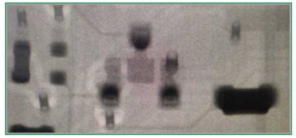
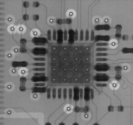
When the x-rays pass through the PCB component, the component’s different densities reduce the x-rays by different amounts. Consequently, light and dark patches are produced on the detection media.
To make this clear, let’s use the example of a solder ball with a minor crack within it. When the x-rays pass through this solder ball, the crack will be easily visible because the solder’s density is greater than that of the air in the crack. This means the solder ball appears in a light area (where the x-rays were attenuated most) with a dark crack (the x-rays were attenuated the least).
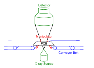
Let’s go further in demonstrating how x-ray for PCB inspection works. Typically, the x-ray source is placed under the lead-lined chamber, and the digital media detector is placed directly above it. A conveyer belt takes the PCB component into the lead-lined chamber and places it (PCB Component) on the manipulator found between the detector and the source.
Once this arrangement is achieved, the X-ray system can then do a detailed inspection of PCB components by manipulating them accordingly.

X-Ray PCB Inspection Techniques
X-ray PCB inspection applies two primary techniques. These are the 2D system and the 3D system techniques.
Let’s now look at what these techniques entail.
- 2D X-Ray System
In this technique, the system produces x-rays at a single point, passing through the PCB component. This way, the system generates 2D images on the media detector. It’s important to note that the 2D systems can be operated either online or offline.
Additionally, the 2D x-ray systems display the whole component’s 2D image from both sides of the PCB.
- 3D X-Ray Systems
If you have a complex double-sided PCB, then the 3D X-ray inspection system is the best option. In this system, the media detector goes through 180-degree circular movement creating images of various cross-sections.
The beauty of this inspection system is that it allows you to focus on specific components at a time. This means that you get a more detailed and precise analysis of the component under inspection.
Benefits of X-Ray for PCB Inspection
- Quick feedback in the early stages of product development enables the manufacturers to take corrective measures to enhance product quality and encourage a positive brand name.
- Designers will have the opportunity not to build on defective parts, saving on unnecessary costs.
- The x-ray enables inspectors to identify a range of potential problems on the printed circuit board and recommend specific corrective actions.
Why Uni X-Ray
Uni X-ray Technology Ltd, based in Shenzhen, China, has almost 20 years of focusing on the design, production, development, and R&D of industrial x-ray machines that are user-friendly and affordable. With years of experience in producing X-ray inspection technology and equipment, Uni X-ray company stands out as a first-class quality solution provider to your manufacturing process.
As a professionally tested and accredited company, Uni X-ray has continued to grow a list of dedicated elite enterprises. With such trust and loyalty, our commitment to customer experience remains our top priority.


