LEDs are increasingly being used as energy saving light sources as a response to new energy regulations. They have decisive advantages over conventional lights: they consume less energy, have longer lifetimes, and are available in various colors. For example, thanks to LEDs, the largest church in the world, St. Peter’s Basilica in Rome, can now be seen in a new light. Via an intelligent control system, even the smallest details of its important treasures can be illuminated with preset lighting scenarios. These digitally controlled systems integrate programmable LED drivers, with which the LEDs can be activated as desired. Figure 1 shows an example of a 3-channel LED driver configuration.
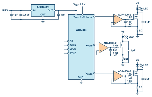
Each of the three output voltages of the digital-to-analog converter (DAC), in this case the AD5686 from Analog Devices, Inc. (ADI), controls a voltage-to-current converter stage in whose load path the individual LED is situated for each LED channel. All three converter stages are realized by an operational amplifier (op amp), ADA4500-2, and a connected MOSFET, which controls the LED current. This LED current can theoretically be up to several amps, depending on the voltage source (VS) and the load resistance, which is 2 Ω in this circuit. Thus, the selection of a suitable MOSFET is very important.The quality of the DAC output voltages is strongly dependent on the reference voltage source VREF. A high quality reference source should be used. The ADR4520 is one such example, as shown in Figure 1. It offers very low noise, extremely high and long-term accuracy, and high temperature stability.
Due to ADR4500-2’s internal design, typical rail-to-rail amplifiers exhibit a certain nonlinearity and crossover distortion. Their input stage consists of two differential transistors connected in parallel: a PNP stage (Q1 and Q2) and an NPN stage (Q3 and Q4), as shown in Figure 2.
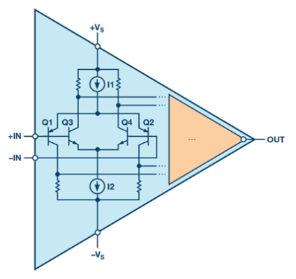
Depending on the applied common-mode voltage, the two input pairs yield different offset voltages and bias currents. If a common-mode voltage is applied to the amplifier input that differs by less than 0.7 V from the negative or positive supply voltage (VS), only one of the two input stages will be active. Then only the error (offset voltage and bias current) of the respectively active stage will appear. If the voltage rises to 0.8 V, both input stages will be active. In this case the offset voltage can change abruptly, leading to so-called crossover distortion and nonlinearity.
In contrast, the ADA4500-2 has an integrated input-side charge pump, which makes it possible to cover the rail-to-rail input range without a second differential pair and thus avoid crossover distortion. Other advantages of the ADA4500-2 are its low offset, bias current, and noise components.
In such circuits, it is important that attention be paid to inductance in the load/current path, which can arise through the wiring of the LEDs. The wires are often several meters long and could cause undesired oscillations if correct compensation is not provided. The compensation in this circuit is achieved by a feedback path that returns the current, measured by a shunt resistor, to the input of the op amp. The existing resistor and capacitor circuitry on the ADA4500-2 should be adjusted according to the arising inductance.
With the circuit shown in Figure 1, a multichannel LED driver that can be programmed via a DAC for precise lighting control applications can be realized relatively easily. However, it is important to adapt the dimensioning to the specific requirements to avoid malfunctioning.

Conclusion
The circuit described in this article shows a relatively easy way to create a programmable LED driver that is ideal for precise lighting control applications that require a compact, scalable, easy to power, and highly linear power source. However, the dimensions must be adapted to the requirements of the application in order to avoid any malfunction due to the various present inductivities, such as line and parasitic inductivity.


