


“New and future SiC/GaN power switches will fuel great advances in everything from significantly greater amounts of next-generation renewable electricity to the rapidly growing market of electrically powered cars. The tremendous benefits of improved power density, higher working frequencies, increased voltages, and better efficiency will deliver more compact and cost-effective power applications. To gain all of these advantages, a much higher performance switch driving system must be designed. The actual switch-centric view is evolving to a much more complete system solution approach, where the next generation of advanced gate driver ICs with much more robust on-board isolation, sensing ICs, power supply controllers, and highly integrated and embedded processors will manage the complex multilevel, multistage power loops required to properly exploit the promise that the next generation of SiC/GaN power converters offer.”
Power converter designs are moving from pure silicon IGBT to SiC/GaN MOSFETs across a variety of applications. Some markets, like the motor drive inverter market, are slower to adopt new technology, while others, like markets for solar inverters and electric vehicle traction inverters and chargers, are playing a key role in innovation.
The solar market is projected to grow with a very positive CAGR of 10% for the next five years, while PV system prices are expected to decrease another 20%. This will be possible due to, and driven by, the technological improvements of PV inverter electronic components. The new technologies in power switches (SiC/GaN MOSFETs) will increase switching frequencies—reducing inductor and capacitor sizes while requiring more accurate, fast, and energy efficient sensing, control, and driving ICs. 1500 VDC utility scale string inverters, in the range of 30 kW to 100 kW, are going to gain more than 90% market share of all utility scale inverters by the year 2021. They represent the benchmark for testing new high density SiC/GaN power switches in innovative multilevel topologies.
Disruptive new applications, like electric vehicles (EVs) and energy storage systems (ESS), are creating demand for ultra-efficient, high power density, high frequency SiC power converters. On-board traction motor drives are looking at the highest power density to reduce size and weight and gain new efficiency records, while off-board fast chargers are seeking for high voltages (up to 2000 VDC, >150 kW) and complex high frequency topologies, resulting in a total system cost reduction on magnetics, mechanics, and assembly. On top of that, these new applications are also pushing the developments of innovative, multicore control processors, and are able to manage complex control algorithms and assure system efficiency and stability when working in bidirectional mode—from the ac grid to the dc load and vice versa.
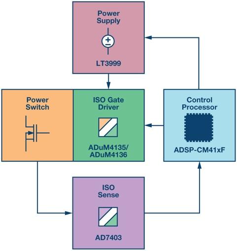
Figure 1. Analog Devices’ IC ecosystem.
Driving SiC/GaN power switches involves designing a complete ecosystem of ICs that are accurately fine-tuned together. The design focus is no longer only switch-centric—it must be more expansive. The application’s working frequencies, efficiency requirements, and complexity of topology require a best-in-class isolated gate driver (for example, ADuM4135) powered by a high end, isolated power supply circuit (for example, LT3999). The control has to be done with a multicore control processor, incorporating an advanced analog front end and specific safety features (for example, ADSP-CM419F). Finally, the compactness of the design is achieved through sensing voltages with energy efficient, isolated Σ-Δ converters (for example, AD7403).
During the transition phase from Si IGBTs to SiC MOSFETs, mixed topologies have to be considered in which SiC MOSFETs are used for the high frequency switches and the Si IGBTs for the low frequency switches. Isolated gate drivers must be able to drive switches with different requirements, with more of them in parallel and in mixed silicon IGBT/SiC MOS multilevel configurations. Customers would like to have one part number meeting the requirements of all their applications, simplifying the BOM and cutting costs. High working voltages, greater than 1500 VDC (for example, 2000 VDC for large scale energy storage), are easy to reach with multilevel converters, and they represent a significant challenge for the isolation barriers that are implemented for safety.
Utilizing Analog Devices’ proven iCoupler® technology, the ADuM4135 isolated gate driver offers a number of key benefits in high voltage and high switching speed applications. ADuM4135 is the best choice for driving SiC/GaN MOS, thanks to a superior propagation delay of better than 50 ns with channel-to-channel matching of less than 5 ns, common-mode transient immunity (CMTI) of better than >100 kV/μs, and the capability to support lifetime working voltages of up to 1500 VDC in a single package.
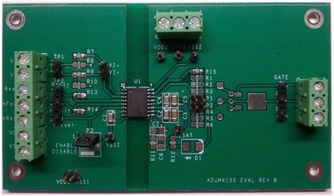
Figure 2. ADuM4135 evaluation board.
The ADuM4135, in a 16-lead, wide-body SOIC package, includes a Miller clamp to provide robust SiC/GaN MOS or IGBT turn-off with a single-rail supply when the gate voltage drops below 2 V. Operation with unipolar or bipolar secondary supplies is possible. Integrated onto the ADuM4135 is a desaturation detection circuit that provides protection against high voltage, short-circuit switch operation. The desaturation protection contains noise reducing features, such as a 300 ns masking time after a switching event to mask voltage spikes caused by initial turn-on. An internal 500 µA current source allows low device count and the internal blanking switch allows the addition of an external current source if more noise immunity is needed. The secondary UVLO is set to 11 V, with common IGBT threshold levels taken into consideration. Analog Devices’ iCoupler chip-scale transformers also provide isolated communication of control information between the high voltage and low voltage domains of the chip. Information on the status of the chip can be read back from dedicated outputs. The primary side of the device controls resetting the device after a fault on the secondary.

Figure 3. ADuM4135 block diagram.
For more compact, pure SiC/GaN-based applications, the new ADuM4121 isolated gate driver is the solution. Also based on Analog Devices’ iCoupler digital isolation, the driver features the lowest-in-class propagation delay of 38 ns, allowing for the highest switching frequencies and the highest common-mode transient immunity of 150 kV/μs. ADuM4121 provides 5 kV rms isolation in a wide-body, 8-lead SOIC package.

Figure 4. ADuM4121 block diagram.
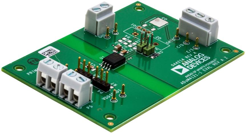
Figure 5. ADuM4121 evaluation board.
When used in high speed topologies, isolated gate drivers have to be powered properly to keep their performance levels. Analog Devices’ LT8304/LT8304-1 are monolithic, micropower, isolated flyback converters. By sampling the isolated output voltage directly from the primary side flyback waveform, the parts require no third winding or isolator for regulation. The output voltage is programmed with two external resistors and a third optional temperature compensation resistor. Boundary mode operation provides a small magnetic solution with excellent load regulation. Low ripple burst mode operation maintains high efficiency at a light load, while minimizing the output voltage ripple. A 2 A, 150 V DMOS power switch is integrated, along with all the high voltage circuitry and control logic into a thermally enhanced 8-lead SO package. The LT8304/LT8304-1 operates on an input voltage range of 3 V to 100 V and delivers up to 24 W of isolated output power.
Analog Devices’ LT3999 is a monolithic, high voltage, high frequency dc-to-dc transformer driver providing isolated power with a small solution footprint. With a maximum switching frequency of 1 MHz, external sync capability, and wide input operating range from 2.7 V to 36 V, LT3999 represents the state of the art for making stable, controlled harmonics and an isolated power supply for high speed gate drivers. It comes in 10-lead MSOP and 3 mm × 3 mm DFN packages with an exposed pad.
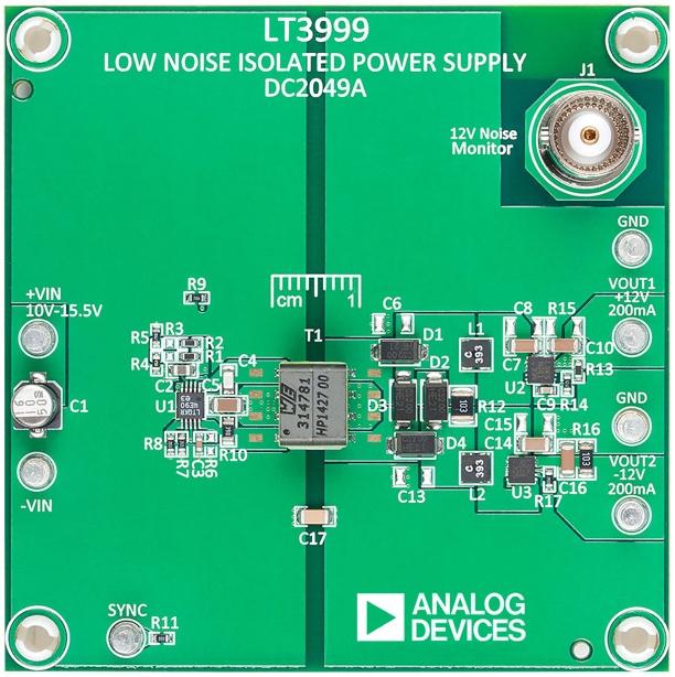
Figure 6. LT3999 evaluation board.
The system control units (generally a combination of MCUs, DSPs, or FPGAs) must have the capabilities of running multiple, high speed control loops in parallel, and also be able to manage the safety features. They have to provide redundancy and a large number of independent PWM signals, ADCs, and I/Os. Analog Devices’ ADSP-CM419F enables designers to have one mixed-signal, dual-core processor managing parallel high power, high density, mixed switch, multilevel power conversion systems.
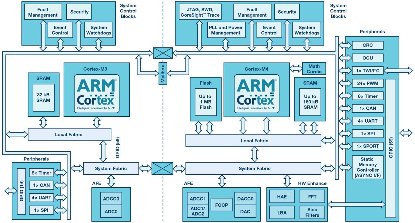
Figure 7. ADSP-CM419F block diagram.
ADSP-CM419F is based on the ARM® Cortex®-M4 processor core, with floating-point unit operating at frequencies up to 240 MHz, and it incorporates an ARM Cortex-M0 processor core operating at frequencies up to 100 MHz. This enables the integration of dual-core safety redundancy into a single chip. The main ARM Cortex-M4 processor integrates 160 kB of SRAM memory with error check and correction (ECC), 1 MB of flash memory with ECC, accelerators and peripherals optimized for power converter control (including 24 independent PWMs), and an analog module consisting of two 16-bit SAR-type ADCs, one 14-bit on M0 ADC, and one 12-bit DAC. The ADSP-CM419F operates from a single voltage supply, generating its own internal voltage supplies using internal voltage regulators and an external pass transistor. It comes in a 210-ball BGA package.
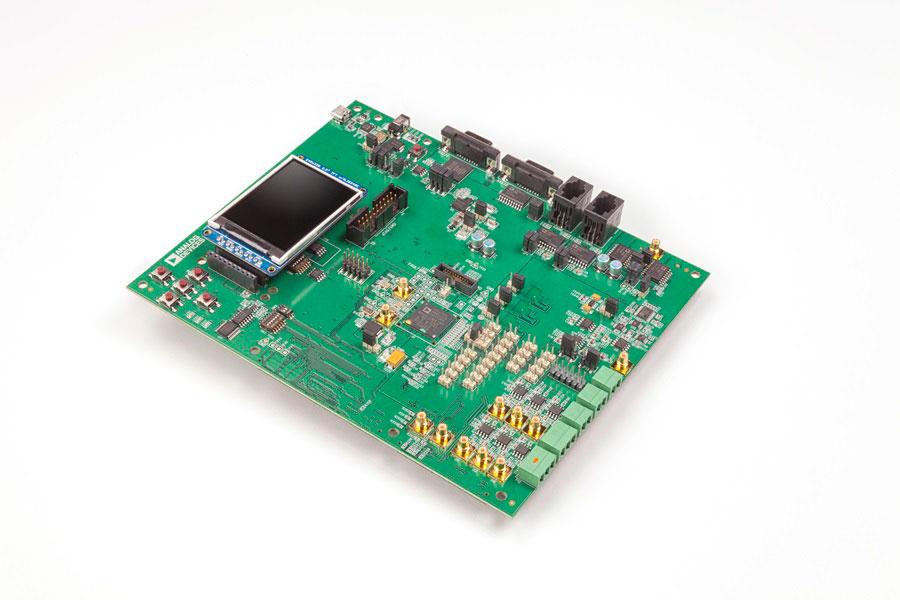
Figure 8. ADSP-CM419F evaluation board.
Fast and accurate voltage sensing is mandatory in high speed designs. Analog Devices’ AD7403 is a high performance, second-order, Σ-Δ modulator that converts an analog input signal into a high speed (up to 20 MHz), single-bit data stream. It combines high speed, complementary metal oxide semiconductor (CMOS) technology with monolithic transformer technology (iCoupler technology) in an 8-lead, wide-body SOIC package. AD7403 operates from a 5 V power supply and accepts a differential input signal of ±250 mV. The original information can be reconstructed with an appropriate digital filter to achieve 88 dB signal-to-noise ratio (SNR) at 78.1 kSPS.
To enable customers’ next-generation power converter designs with high performance, reliability, and market competitiveness, Analog Devices decided to develop various hardware and software design platforms that can be used for both evaluating the ICs and as a building block for the complete system. Currently targeted at strategic customers, the design platforms represent the state of the art for showing the complete IC ecosystem for driving next-generation SiC/GaN power converters. They vary from isolated gate driver boards for high voltage, high current SiC power modules to complete ac-to-dc bidirectional converters where the software for ADSP-CM419F plays a key role in properly controlling the SiC/GaN power switches.


