Fully Depleted Silicon on Insulator (FD-SOI) has matured over time and emerged as a boon for low-power semiconductor design. STMicroelectronics was the first company to commercialize an FD-SOI process, which was later licensed to Global Foundries. Our editor Pratibha Rawat, had a candid interview with Andreia Cathelin, Technology R&D Fellow, STMicroelectronics in which she talks about the FD-SOI technology and how ST is progressing towards the FD-SOI ecosystem.
What differentiates FD-SOI as an important process technology?
Andreia Cathelin: FD-SOI is, in many respects, an evolutionary process technology to most design engineers: the transistor devices are fully depleted (as in FinFETs), but they are planar devices like the previous regular CMOS generations. This planar structure supports the use of the same EDA design tools as for regular CMOS, to which circuit designers are fully accustomed and well trained, so the retooling and re-learning for the system and design flows is really minimal.
What is the potential advantage of FD-SOI over the FinFET technology?
Andreia Cathelin: FD-SOI has numerous advantages over FinFET technology. One important consideration is that it is by construction more energy efficient, which allows it to run cooler, That has a compounding effect, as it generates less heat, so it runs longer or alternatively permits battery saving. FD-SOI can also be body biased very efficiently over a very large voltage tuning range, which allows circuits to be tuned either for faster performance or for lower power consumption. Finally, FD-SOI is a planar technology, so unlike FinFETs, which are vertical structures that require EDA and process retooling, FD-SOI uses a style of design that is familiar to most engineers.
Can we say, the MOU between ST and GF will find a solution for the semiconductor shortage and What else this partnership will bring out?
Andreia Cathelin: ST and GF have signed the MOU on the jointly owned, high-volume manufacturing facility to support European and global customers’ demand as the world transitions to digitalization and decarbonization. The new facility will strongly contribute to the objectives of the European Chips Act, including the goal of Europe reaching 20% of worldwide semiconductor production by 2030. It will also support ST’s $20+ revenue ambition and, by working with GF, we can go faster, lower the risk thresholds, and reinforce the European FD-SOI ecosystem.
ST was an early innovator in FD-SOI and has been in production for several years, with both custom and standard advanced products. What changes have you seen in this technology so far and What are the risks and downsides of FD-SOI?
Andreia Cathelin: FD-SOI technology has origins in the Grenoble, France area. Moreover, it has been part of ST’s technology and product roadmap in our Crolles facility since its early beginnings. FD-SOI offers big benefits to the market, including its ultra-low power consumption, as well as easier integration of additional features, such as RF connectivity, mmWave, and security. FD-SOI is a perfect technology for a full SoC integration for our different families and microcontrollers, including all of their adjacent RF connectivity and service circuits. It permits us to fully serve the IoT market with energy efficient and sustainability-aware solutions.
How is it going to support or contribute to European Chips Act and how this association will support digitalization and decarbonization?
Andreia Cathelin: Among the ambitions highlighted in the European Chips Act are the goal of Europe providing 20% of global semiconductor production by 2030. The new joint fab will also support the leadership and resilience of the European technology ecosystem, including R&D to large-volume manufacturing. It will also assure capacity in complex, advanced technologies for key end-markets, including automotive, industrial, IoT and communications infrastructure. Also, not to be ignored, the new fab will add approximately 1000 new jobs for the manufacturing facility and across the full ecosystem of partners, suppliers, and stakeholders.
ST is advancing towards the FD-SOI ecosystem from R&D (with the recently announced cooperation on R&D among ST, GF, CEA-Leti and Soitec) and now the new joint fab what else industry can expect in this ecosystem?
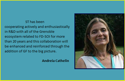
Andreia Cathelin: ST has been cooperating actively and enthusiastically in R&D with all of the Grenoble ecosystem related to FD-SOI for more than 20 years and this collaboration will be enhanced and reinforced through the addition of GF to the big picture.
What role will ST Crolles’s facility play in the new fab?
Andreia Cathelin: The new 300mm semiconductor manufacturing facility is being built adjacent to ST’s existing 300mm facility in Crolles, France. The new site is targeted ramping up from 2024, with ramp to full capacity – 620,000 wafers/week – by 2026.


