


CIRCUIT FUNCTIONS AND BENEFITS
While the world continues to become more digital where compute power and digital functionality are more critical, the need to meas- ure the environment and interact with real-world devices remains an analog function. To operate at the boundary of digital and analog domains, processors must include mixed-signal inputs/out- puts and accommodate more software programmable ranges to be considered for many industrial, instrumentation, and automation applications.
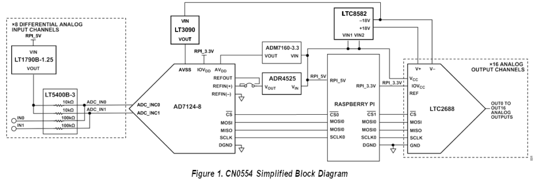
The circuit shown in Figure 1 is a flexible, multichannel mixed-signal analog input/output (I/O) module. The 16 single-ended analog outputs are software configurable, with ranges of 0 V to 5 V, ±5 V, 0 V to 10 V, and ±15 V. Eight channels of fully differential analog input are provided with hardware selectable input ranges of 0 V to 2.5 V, ±13.75 V, and 0 V to 27.5 V.
The circuit is designed to mount directly on top of a Raspberry Pi, providing this popular single board computer an analog I/O interface. Software control is accessible through the Linux industrial input/output (IIO) framework, providing a host of debug and development utilities, cross-platform application programming interface (API) with language bindings for C, C#, MATLAB, Python, and more.
The software can run either locally on the Raspberry Pi or can be controlled remotely via a wired or wireless network connection. The 5 V power for the module is supplied via the Raspberry Pi interface connector, no additional power source is required. All these features make the system suitable for low power, local and remote, precision analog I/O applications.
CIRCUIT DESCRIPTION
The CN0554 provides a complete analog I/O system for precision applications. The circuit can be subdivided into two main components, the analog-to-digital conversion (ADC) and the digital-to-analog conversion ( DAC ).
ANALOG INPUTS
The CN0554 can accommodate analog input voltage range up to 11 times of input attenuation through the on-board LT5400 external matched resistor network. This device increases the analog input voltage range via jumper selection.
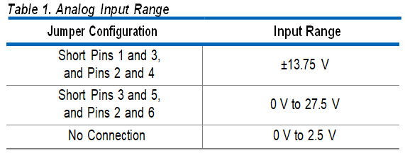
Table 1 presents the complete jumper configuration and corre- sponding analog input voltage ranges for CN0554.
ANALOG-TO-DIGITAL CONVERSION
The CN0554 features the AD7124-8, a 24-bit Σ-Δ ADC with config- urable analog inputs. Eight channels of the fully differential inputs or 16 single-ended input channels can be configured software, along with the programmable gain, filter settings, and output data rate.
The external voltage reference is jumper-selectable to either the internal band gap reference of the AD7124-8 or the 2.5 V output of the ADR4525, a high precision, low power, and low noise voltage reference. As the reference voltage drift directly impacts the accura- cy of the ADC, the CN0554 uses an external reference because it exhibits a better temperature drift performance compared to an internal reference.
The Σ-Δ architecture of the AD7124-8 provides high resolution and noise rejection in small-signal sensor measurements, and even in high noise environments such as industrial settings. The output data rate is programmable from 1.17 SPS to 19.2 kSPS, with corresponding measurement resolutions from 24 nV rms to 72 μV rms, respectively; and several filter modes are available. This allows the resolution, data rate, and noise rejection of the CN0554 to be optimized for a wide range of applications.
DIGITAL-TO-ANALOG CONVERSION
The CN0554 features 16 single-ended, 16-bit analog outputs using the LTC2688 voltage output DAC. Each channel has an internal rail-to-rail output buffer that can source or sink up to 20 mA.
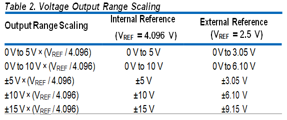
An LT8582 provides ±18 V supply rails to the LTC2688, allowing the DAC to fully utilize its analog output range up to ±15 V. The output range of each channel is independently programmable to five ranges listed in Table 2. The voltage reference is software programmable to use either the internal 4.096 V or the ADR4525 2.5 V reference used for the ADC. Each channel also supports 5% overrange.
TOGGLE AND DITHER FUNCTIONALITY
The CN0554 supports both toggle and dither capabilities. The toggle function enables fast switching of a DAC output between two different DAC codes without any SPI transaction, thereby elim- inating communication transactions. Examples include injection of a small dc bias, or independently switching between on and off states.
Dithering reduces quantization error in precision applications and is done by spreading nonlinearities across several output codes. This function is useful in many applications requiring the ac signal to be superimposed around the average dc value of a signal. One example is in optical applications wherein the secondary characteristic of an optical path can be measured by its response to a small ac signal. Moreover, dither reduces stiction in mechanical systems such as spool valves, speeding up response when the position of the spool is changed.
Toggle Operation
As shown in Figure 2, each channel supports the toggle operation which allows controlled switching of the output voltage between two values set through software. The switching is controlled by a toggle signal, which can be sourced from one of three different external digital inputs (designated as TGP0, TGP1, and TGP2) from the Raspberry Pi or an internal software-controlled register. Two of the three digital signals, TGP0 and TGP1, connect to Raspberry Pi digital outputs, which support pulse-width modulation (PWM).
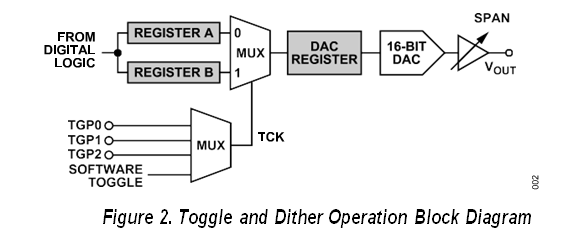
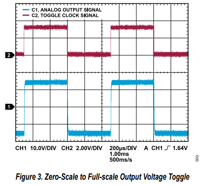
Figure 3 displays an example toggle operation performed by the CN0554. The output voltage swings between zero-scale and full- scale values in response to the toggle pins, with measured peak-to- peak voltage of 33.0 V at 1 kHz.
Dither Operation
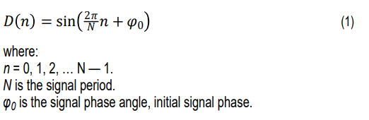
In CN0554, each channel also supports the dither operation which adds a sinusoidal dither signal to the analog output. The sinusoid is generated using a lookup table with values from Equation 1
The CN0554 allows configuration for the dither signal’s amplitude, period, and phase angle.
The amplitude of the dither signal is set through software and can range from 0 to 25% of the set maximum output voltage.
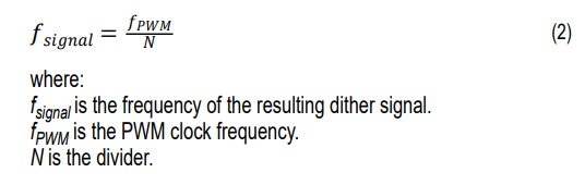
To set the dither frequency, a dither clock input is required and selectable from any of the three external digital inputs, TGP0, TGP1, and TGP2, from the Raspberry Pi. Two of the external inputs, TGP0 and TGP1, are connected to Raspberry Pi digital outputs with a PWM feature allowing for easy configuration of the clock frequency. The frequency of the dither signal is set from the dither clock input divided by a software configurable divider of 4, 8, 16, 32, and 64, such that the frequency of the resulting dither signal is computed using Equation 2
The dither phase angle is configurable to four different values: 0, 90, 180, and 270. All these parameters enable precise control of dithered DAC channel outputs.
Figure 4 shows an example dither operation performed by the CN0554 at mid-scale output voltage for maximum signal period, with peak-to-peak voltage of 15.04 V at 1 kHz dither clock.
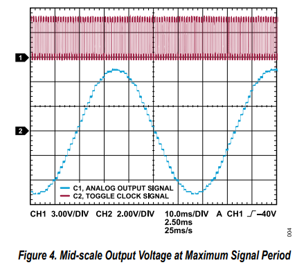
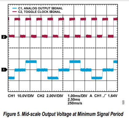
Figure 5 shows the dither operation at mid-scale output voltage for minimum signal period, with peak-to-peak voltage of 17.6 V at 1 kHz dither clock.
SYSTEM PERFORMANCE
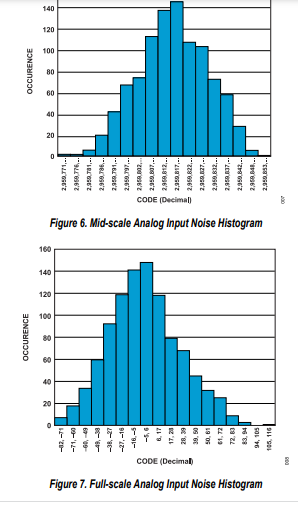
Analog Input Noise Performance
Figure 6 shows the noise characteristics at a mid-scale input (5 V) and Figure 7 shows the noise characteristics at a full-scale input (10 V).
Analog Output Noise Performance
The switching regulator outputs of the LT8582 are bypassed and filtered to reduce noise. Figure 8 shows the ac-coupled signal noise at zero-scale output, which exhibits the lowest peak-to-peak noise at 14.4 mV.
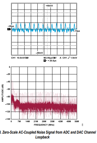
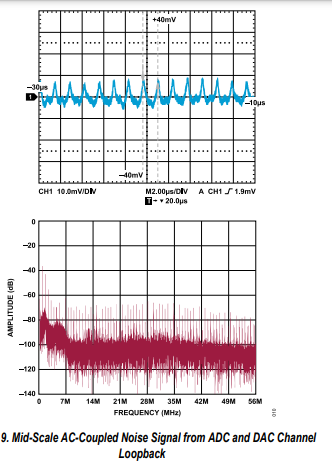
Figure 9 presents a peak-to-peak noise of 13.4 mV taken at mid- scale output.
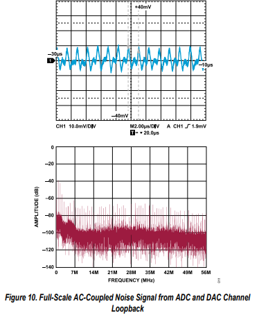
In Figure 10, the board generates the highest peak-to-peak noise of 17.6 mV at full-scale output.
Analog Output Linearity
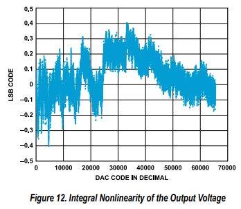
Integral nonlinearity (INL) is the measurement of the maximum de- viation, in LSBs, from a straight line passing through the endpoints of the DAC transfer function. Moreover, differential nonlinearity (DNL) is the difference between the measured change and the ideal 1 LSB change between any two adjacent codes. A specified differential nonlinearity of ±1 LSB maximum ensures monotonicity.
Figure 11 shows the DNL measured in LSBs of the output voltage compared to the 16-bit set value to the LTC2688 output for a single channel.
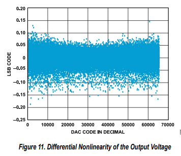
Figure 12 shows the integral INL measured in LSBs of the output voltage compared to the 16-bit set value to the LTC2688 output for a single channel.
POWER ARCHITECTURE
The CN0554 derives power directly from the Raspberry Pi 40-pin interface connector. Figure 13 shows the complete power tree of the CN0554.
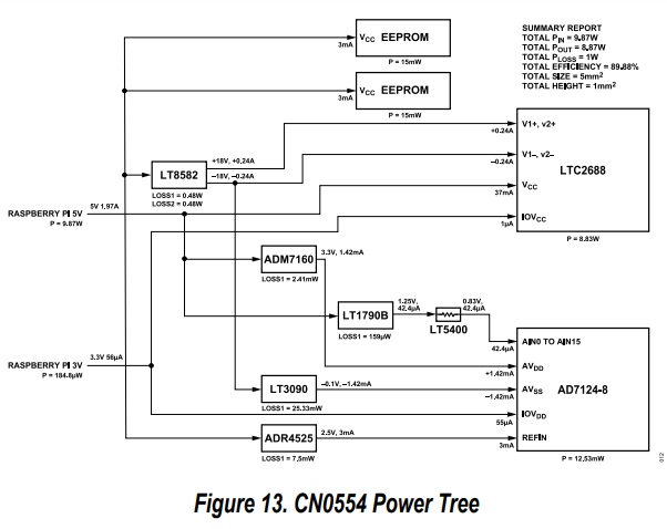
The LT8582, a dual independent channel switching dc/dc converter, is responsible for boosting and inverting the 5 V power coming from the Raspberry Pi.
The LT8582 outputs 18 V and -18 V rails, which are then used to provide the necessary power rails for both the ADC and DAC. The CN0554 also offers input overvoltage and overtemperature protection through the fault protection feature of the LT8582.
An ADM7160, ultralow noise, low dropout regulator provides the 3.3 V analog supply rail for the AD7124-8. The regulator is powered from the 5 V rail on the Raspberry Pi interface connector. The AD7124-8 digital I/O supply is tied directly to the 3.3 V rail of the Raspberry Pi.
The LT3090 regulates the -18 V rail to -0.1 V, providing a slightly negative analog supply for the AD7124-8. The supply rails were designed such that the absolute analog input voltage can span the entire range from ground to the reference voltage even with the input buffers enabled.
COMMON VARIATIONS
The AD7124-4 can be used in place of AD7124-8, with only 8 single-ended and/or 4 differential channels; this brings down the cost for applications not requiring the extra channels.
The LTC2686 is an 8-channel alternative for the LTC2688. It has a higher output drive current at 55 mA and compensation pins for driving high capacitive loads.
The LT8582 can be replaced with a single, positive 5 V supply if only 0 V to 5 V output ranges are required. Alternative supply options for the DAC can consider lower output current boost or
inverting regulators as the board is designed to support full DAC output current on all channels.
Additionally, low noise post-regulation of the boost or inverting regulators such as low dropout voltage regulators can also be added depending on the application.
CIRCUIT EVALUATION AND TEST
This section covers the setup and procedure for evaluating the EVAL-CN0554-RPIZ. For complete details, refer to the CN0554 User Guide.
EQUIPMENT NEEDED
- EVAL-CN0554-RPIZ Circuit Evaluation Board
- Raspberry Pi 4 Model B
- Display monitor with HDMI
- Micro HDMI to HDMI adapter
- USB keyboard and mouse
- 16 GB or larger SD card
- Analog Devices, Inc. Kuiper Linux image
- 5 V, 3 A USB Type-C power adapter
- Female-to-female loopback jumper cables
- Oscilloscope
- Digital voltmeter (6-digit or higher)
GETTING STARTED
The CN0554 evaluation board is by default configured with the correct shunt positions for testing. Visit the EVAL-CN0554-RPIZ User Guide to verify the shunt positions.
To perform the evaluation test, follow the steps below:
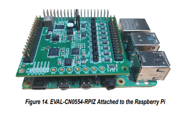
- Connect EVAL-CN0554-RPIZ to the Raspberry Pi, as shown in Figure 14.
- Insert the SD card with Kuiper Linux image into the Raspberry Pi.
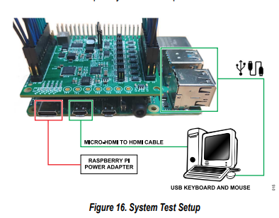
Connect the ADC input and DAC output channels using the female-to-female loopback jumper cables, as shown in Figure 15
- Connect the HDMI cable from the Raspberry Pi to the display monitor, and then connect the keyboard and mouse to the USB ports.
- Power the Raspberry Pi using the USB Type-C power adapter and wait for the Raspberry Pi to boot up.
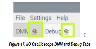
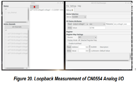
Open IIO Oscilloscope and undock the DMM and Debug tabs as shown in Figure 17
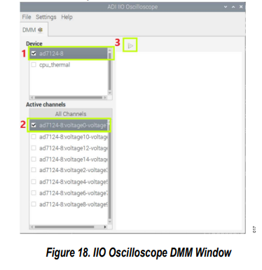
In the DMM Window, select the ad7124 as the device and select a channel to measure, such as ad7124-8:voltage0-volt- age1. Click on the Play button to start the measurement.
In the Debug Window, select ltc2688 in Device Selection. In the IIO Device Attributes section, select output voltage1 channel and select raw attribute. Set the value to 32768 and Click Write. This should set the output voltage to around 2.5 V, which is half of the default output range of 0 V to 5 V.
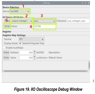
The DMM measurement should show approximately 0.227 V or 1/11 of 2.5 V, which is the default input voltage attenuation.

")


