


Introduction
EV Sales is growing at a faster rate among all the countries and by 2040 it is expected to cross 60 million units. Many countries have plan to shift totally to Electric Vehicles in near future. There are lot of factors which are helping for its growth – global Warming due to the emissions of hydrocarbons, fast depletion of the Fossil fuels, recent surge in high fuel pricing, collaborative Development of Charging standards and Interoperability and increase in Charging infrastructure. With recent advancement of battery technologies promise to deliver vehicles with even longer ranges while reducing battery cost and weight. Also, these new batteries exhibit ever improving charge acceptance, allowing significant faster charging rates. Development made with DC Fast Chargers are key to driving down the charging times and help to get more range distances with reduced range anxiety for the user.
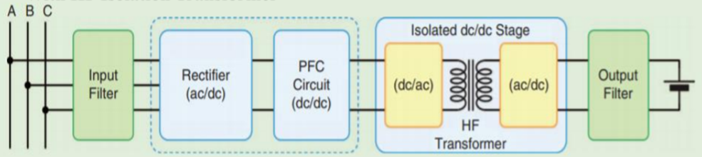
Presently all the off-board charger has two stages – Power Factor Corrector (PFC) and DC-DC Converter stage with isolation provided by the high frequency transformer (Fig 1). The usage of Wide Band Gap Devices (WBG) makes the system operate at high frequency which in turn makes the charger light in weight, lower cost, higher efficiency, and faster charging power; though we are now switching at higher frequency which makes the switching losses dominant.
Vienna Rectifier
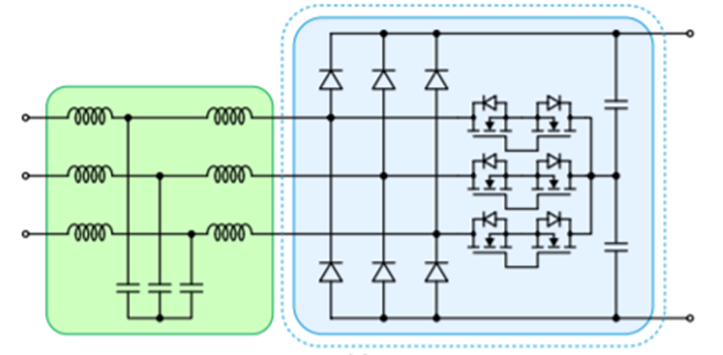
The Vienna rectifier power topology is used in high-power, three-phase power factor correction applications. The Vienna rectifier is popular due to its operation in continuous conduction mode (CCM), inherent multilevel switching (three level), and reduced voltage stress on the power devices (Fig 2). Both hysteresis-based and sine triangle-based controllers have been used for Vienna rectifiers, hence it is relatively simpler to control due to the smaller amount of PWMs required for this topology. One of the drawbacks of this topology is that it only supports unidirectional mode power transfer from the grid to the DC side. Vienna rectifier is characterized by a relatively small overall volume or a high-power density as it requires approximately only half of the inductance for the boost inductors.
The STDES-30KWVRECT reference design introduces a complete digital power solution for high-power three-phase active front end (AFE) rectifier applications based on the three-level Vienna topology (Fig. 3). This platform achieves a peak efficiency of more than 98.5% by using the SCTWA90N65G2V-4 and the STPSC40H12C. It features a fully digital control with the STM32G474RE mixed-signal high performance microcontroller, providing the full control of the PF, DC voltage, and soft startup procedure. The STDES-30KWVRECT achieves a low total harmonic distortion (less than 5% THD at full load) and a high-power factor (higher than 0.99 at full load), providing a high-bandwidth continuous conduction mode (CCM) current regulation.
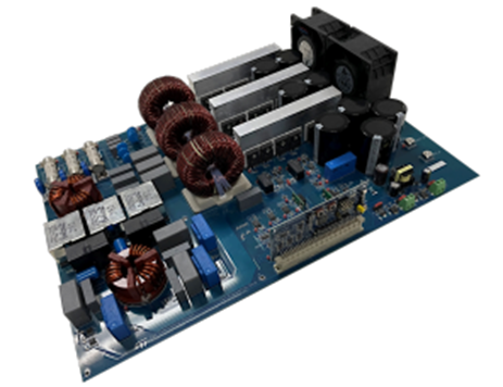
Fig 3: Evaluation Board (STDES-30KWVRECT)
Features of the Evaluation Board (STDES-30KWVRECT)
• Three-phase, three-level AC-DC power converter:
– Nominal rate for DC voltage: 800 VDC
– Nominal rate for AC voltage: 400 VAC at 50 Hz
– Maximum power: 30 kW
– Power factor: >0.99
– Inrush current control and soft start-up
– THD lower than 5% at nominal operation
• Power section based on SiC MOSFETs and SiC diodes:
– High frequency operation (70 kHz)
– High efficiency: >98.5%
– Paralleled SiC MOSFETs for higher power with balanced sharing current
– Passive element weight and size reduction
• Control section based on the STM32G474RE microcontroller:
– Control and monitoring interfaces: SWD–UART, I²C, and DACs
– 64-pin digital power connector
– LED status as UI
– Four integrated high-performance op-amps for additional features
Circuit Scheme for three level Vienna
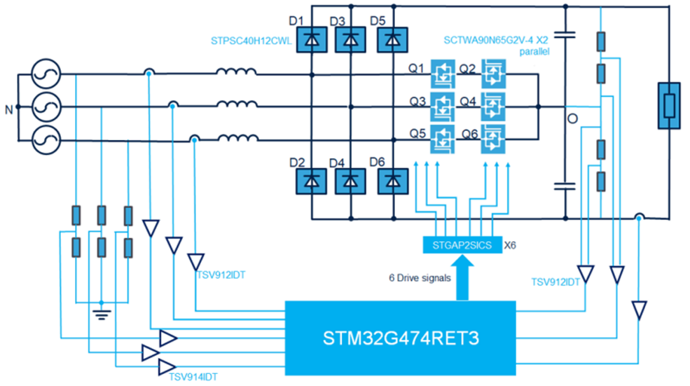
The Vienna rectifier works as a three-phase boost converter that steps up the AC mains input voltage to 800 VDC output while forcing a sinusoidal input current that is in-phase with the input voltage on all three phases. Each phase consists of a boost inductor, a pair of rectifiers (STPSC40H12C SiC Schottky diodes) and a set of series connected MOSFETs (each position uses two paralleled SCTWA90N65G2V-4 SiC MOSFET). The MOSFETs are connected to the center point of a capacitive divider, which reduces the voltage stress on the SiC MOSFETs. Two SiC Schottky diodes of each phase are used for boosting during the input AC voltage positive and negative alternation. The driving circuit is an STGAP2SICS galvanic isolated driver IC for SiC MOSFETs. It provides 4 A driving current capability and a common mode transient immunity (CMTI) up to 100 V/ns.
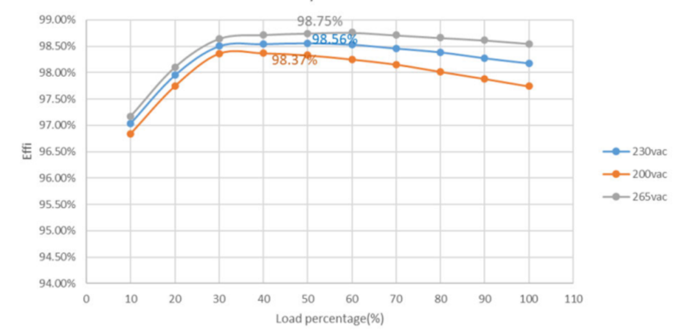
Performance of the PFC Front End
The PFC efficiency measurement under various operating load conditions and different AC input voltage conditions. At 400 VAC (L-L) condition, this reference design provides a 98.56% peak efficiency. At 450 VAC (L-L) condition, the reference design can reach a 98.75% peak efficiency.
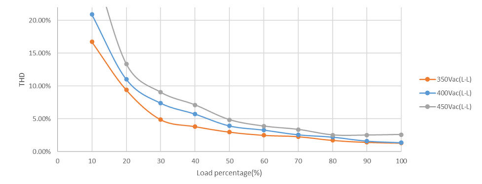
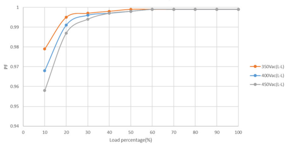
The figures (Fig. 6 and Fig. 7) show the PFC vs iTHD and PF value results under various operating load conditions and different AC input voltage conditions. In the whole AC input voltage range, iTHD is less than 5% when the load is larger than 50%. The PF value reaches 0.998 when the load is larger than 50%.
Dual Active Bridge Converter (DAB)
Dual Active Bridge Converter (DAB) consists of a full bridge with active switches on both the primary and secondary sides connected by a high-frequency transformer (Fig 8). Typically used for EV charging applications due to its high-power density, high-efficiency, buck and boost capability, low device stress, small filter components, and low sensitivity to component variation. The control of the DAB ranges from simple (or single-phase shift modulation) to complex (for extended, dual and triple phase shift modulation). This topology can be used to cover a wide variation of battery voltages with single phase shift modulation but circulating currents in the transformer increase which drastically reduces efficiency. But with advanced modulation schemes like triple phase shift, the converter can theoretically achieve ZVS over the entire operating range.
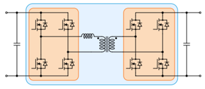
Fig 8: Dual Active Bridge Converter (DAB) Topology
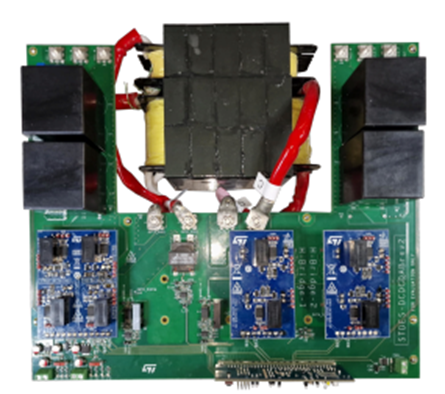
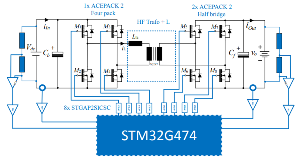
The STDES-DABBIDIR provides a complete solution for a bidirectional DC-DC Power Converter (Fig 9). A dual active bridge topology based on ACEPACK 2 SiC power modules is proposed. The STM32G474RE MCU, enabling digital-intensive power control and optimized for mixed-signal applications, is used. Thanks to the latest generation SiC power module and high-frequency operation (100 kHz), high performance and design optimization are reached. Soft switching DAB behavior is managed by adaptive modulation techniques, according to the load/voltage variation. Bidirectional mode operation supports V2G and V2L implementations as well as UPS and battery energy storage applications.
Features
• Dual active bridge DC-DC power converter
– Nominal DC input voltage: 800 V
– Nominal DC output voltage: 400 V
– Nominal power: 25 kW
– Switching frequency: 100 kHz
– Peak efficiency: 98.4%
• Key features
– ACEPACK 2 SiC power modules to optimize integration and thermal dissipation
– Bidirectional digital power control
– Extended soft switching mode, enabled by sophisticated modulation techniques
– Passive elements weight e size reduction thanks to high frequency SiC MOSFETs operation
– STGAP2SICS galvanic isolated gate driver for SiC
– STM32G474RE MCU for full digital solution
– Inrush current control and soft startup
• Reference design modular architecture
– Main power board
– Driving boards (1xHV side 2xLV side)
– Control board based on STM32G474RE
Circuit Scheme for Dual Active Bridge Converter
The DAB DC-DC stage consists of two full-bridges and a 25 kW single magnetic component, including the
isolation transformer and the inductance. The hardware modular structure includes the following parts:
• A main power board with ACEPACK 2 SiC power modules, an A2F12M12W2-F1 full bridge for the primary
HV side and two half bridges for the secondary LV side. In addition to the power modules, a bulk capacitor,
sensing sections, and an auxiliary power supply are also present.
• A driver board for the ACEPACK 2 full bridge SiC power modules based on the STGAP2SICS galvanically
isolated 4 A single gate driver for SiC MOSFETS.
• Two driver boards for the ACEPACK 2 half bridges SiC power modules based on the STGAP2SICS
galvanically isolated 4 A single gate driver for SiC MOSFETs.
• A control board based on the STM32G474RET3 microcontroller with connectors for communication and
programming, test-points, and status indicators for testing and monitoring.
A dual active bridge, voltage, and current control are proposed for bidirectional power flow according to the
topology characteristics. Soft startup procedure and protections are also managed by the MCU.
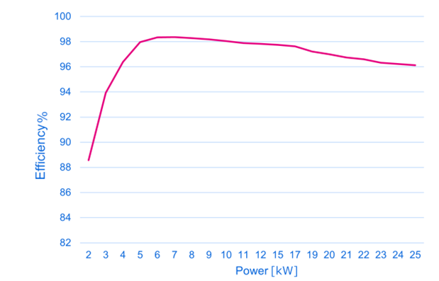
Performance of DAB Converter
The DAB efficiency measurement under varyIng power load. At 800VDC Input and 500VDC output, this reference design provides a 98.4% peak efficiency.

Sr. Technical Marketing Manager, Power Discrete and Sub Analog (PDSA), STMicroelectronics
Conclusion
The demand of high-power converters for charging station is increasing along with the efficient and higher power density. The solution for 30KW can be stacked in modular fashion to increase the power rating so as to have a high charging capacity which is essential, especially if a large number of vehicles is to be charged at the same time in one place The ST Solution of Vienna Type 2 PFC and DAB Converter both achieves peak efficiency of 98%. Using power semiconductors based on silicon carbide optimizes power density, system size, and cost. ST provides a complete kit of devices like SIC Mosfets, SIC Diode, Isolated Gate Drivers, Microcontrollers, Power Management products for designers to develop a complete solution.


