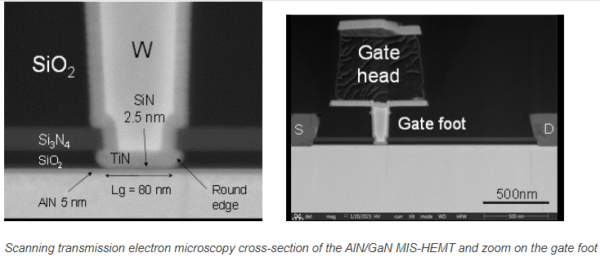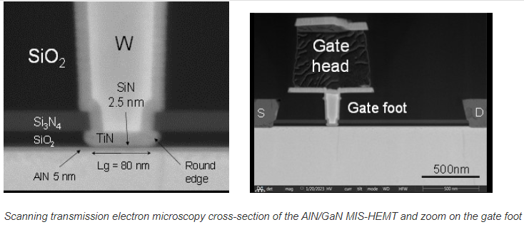
CEA-Leti has developed a 200mm gallium nitride/silicon (GaN/Si) process technology compatible with CMOS cleanrooms that preserves the high performance of the semiconductor material and costs less than existing GaN/SiC technology.
In one of nine presentations at IEDM 2023, the institute said that current GaN high-electron-mobility-transistor (HEMT) technologies used in telecom or radar applications come on small GaN/SiC substrates and require processing in dedicated cleanrooms.
The high-performance SiC substrates used to grow GaN layers are very expensive and available only in relatively small size. This R&D project developed GaN/silicon technology (GaN/Si) on 200mm and later for 300mm wafer diameters in CMOS-compatible cleanrooms to reduce substrate cost and benefit from existing high-performance cleanroom facilities.
As a result, CEA-Leti’s GaN/Si technology performance at 28 GHz is gaining ground on GaN/SiC technology in terms of power density.

“Our goal was to reach existing state-of-the-art GaN HEMT performance at ~30 GHz with a 200mm CMOS- compatible GaN/Si technology and to compete with GaN/SiC technology,” said Erwan Morvan, CEA-Leti scientist and lead author of the paper, “6.6W/mm 200mm CMOS Compatible AlN/GaN/Si MIS-HEMT with In-Situ SiN Gate Dielectric and Low Temperature Ohmic Contacts”.
“This work demonstrates that CMOS-compatible 200mm SiN/AlN/GaN MIS-HEMT on silicon technology is a promising candidate for applications like 5G/6G infrastructure, satcom, radar for UAV detection or earth observation. It should enable less expensive devices while keeping high power density, high efficiency, light weight and compactness,” he said.
The devices developed in this work, which are designed for RF amplifiers and switches, can be used in those applications around 30 GHz.
While reliability testing on the process technology is just beginning, CEA-Leti’s ongoing R&D in this area will include increasing the raw output power and efficiency of its MIS-HEMT transistors, integrating its improved process modules to boost device performance & increase operation frequency toward 100+ GHz, and 3D integration of GaN/Si chips on 300mm Si wafers.


