Abstract
Consumers expect hearables, wearables, and other ultra-small electronic devices to be long on battery life despite their tiny form factor. Yet, clearly, the device size does limit the battery capacity. This paper discusses how to gain some of that space back by using a switching regulator based on a single-inductor multiple-output (SIMO) power converter architecture. The SIMO architecture, along with the regulators’ low quiescent current, enable the IC to extend battery life for space-constrained electronic products.
This paper will help you gain a deeper understanding of SIMO technology and how it works. You will also learn about power management ICs (PMICs) featuring the SIMO regulator that reduce power dissipation and overall component count, while providing the same functionality of traditional solutions in less than half the space.
Introduction
Meeting the Battery Life Demands of Tiny Devices
When you put in your earbuds for a long hike or an afternoon working on a big project, you don’t want to be interrupted by having to stop and recharge the earpieces. You expect your hearables, wearables, and other tiny, battery-powered electronic devices to perform reliably over long periods of time.
From a design standpoint, these user expectations are a tall order to meet. The form factor constraints dictate the need for a small Li+ battery, which must last a long time between charge cycles and be utilized sparingly. Power supplies, in turn, must meet the distinct and diverse voltage requirements of the sub-systems within the design.
The SIMO architecture provides an optimal solution for these systems, integrating functionality that would otherwise require multiple discrete components. Let’s take a closer look at what a SIMO architecture is and how it works for buck-boost regulators.
SIMO Architecture Overview
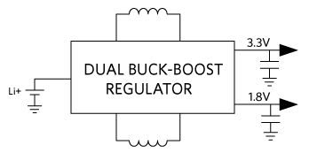
In a traditional switching-regulator topology, each switching regulator needs a separate inductor for each output (Figure 1) since each voltage rail must be serviced by an individual inductor. The inductors are physically large and costly, so this is a disadvantage for small form factor products. Linear regulators offer another option—they are fast, compact, and low noise, but they are also lossy. There’s also the hybrid alternative of using multiple low-dropout regulators (LDOs), in conjunction with DC-DC converters. However, while this configuration would result in intermediate power and heat dissipation, it still yields a larger design than LDOs alone.

Figure 1. Traditional architecture for a buck-boost switching regulator.
The featured buck-boost SIMO converter can regulate up to three output voltages over wide output voltage ranges using a single inductor. The buck-boost topology helps to better utilize the inductor since it requires less time to service each channel as compared to a buck-only SIMO. The weakness of a buck-only SIMO is magnified as one or more output voltages approaches the input voltage. A buck-only SIMO will suffer when an output voltage approaches the battery voltage. At this time, a buck-only SIMO requires the inductor for too much time, which impacts other channels.
Sometimes, an inductor cannot be avoided in the system. Even though they are small, an LDO can never provide a boost feature by itself. Since the SIMO requires only one iductor, solutions that require at least one boost voltage are almost always better with a buck-boost SIMO.

Figure 2. SIMO architecture block diagram.
The inductor saturation current (Isat), a measure of the inductance drop to a certain percentage that corresponds to a particular electrical current, is proportional to the inductor’s core size for a given core material and construction. Using one inductor in a SIMO architecture offers various advantages versus using separate DC-DC converters:
- When allowed by the system, you can better utilize Z-height
- Cost savings and footprint are improved since you don’t have to use as many inductors as compared to the traditional solution
- Time multiplexing, when different features are often not used simultaneously. This benefit manifests when the total supply current is less than the sum of the individual output requirements. For example, you might have events that happen sequentially using different rail voltages. In some Bluetooth systems, for instance, data can be downloaded before it activates a function. That means the power associated with the radio are on at different times than the activated function(s). Thus, the total Isat required for the SIMO inductor is less than would be required for separate converters.
- RMS (current rating for inductors)—even though channels are not time-multiplexed, the peak power consumption of features often doesn’t happen at the same time, which can also lower the total inductor Isat requirements
Overcoming SIMO Architecture Compromises
Using a SIMO architecture is not without tradeoffs. As such, a thoughtful approach to the design is important. For example, the output voltage ripple will often be higher because there is a single inductor providing buckets of energy to alternate outputs. Also, as a SIMO is heavily loaded, it becomes time-limited and there can be delay in servicing each channel, which can further increase output voltage ripple. Using larger output caps offsets these sources of output voltage ripple while maintaining a net footprint/BOM advantage.
New power management ICs (PMICs) from Maxim, the MAX77650 and MAX77651, provide a careful balance of these tradeoffs. These PMICs were designed with micropower SIMO buckboost DC-DC converters. An integrated 150mA low-dropout regulator (LDO) in the PMICs provides ripple rejection for noise-sensitive applications such as audio. Optional resistors (24Ω) in series with serial data line (SDA) and serial clock line (SCL) minimize crosstalk and undershoot on bus signals, while also protecting device inputs from high-voltage spikes on the bus lines. Every block in these regulators has low quiescent current (1µA per output), which helps extend the end application’s battery life. Since the IC always operates in discontinuous conduction (DCM) mode,the inductor current goes to zero at the end of each cycle to further minimize crosstalk and prevent oscillation.
The SIMO converter utilizes the whole battery voltage range, as each output has the benefit of being a buck-boost configuration, which creates output voltages that are above, below, or equal to the input voltage. Since peak inductor current for each output is programmable, you can optimize the balance between efficiency, output ripple, electromagnetic interference (EMI), PCB design, and load capability. Efficiency on these ICs is rated at more than 85% at 3.3V output.
This SIMO architecture finds the optimal balance between low power consumption and form factor. The low power consumption can be very important for very small applications that are unable to dissipate much heat. Figure 3 illustrates how the MAX77650 PMIC is optimal in terms of heat dissipation and form factor compared to configurations utilizing DC-DC converters with multiple LDOs or simply multiple DC-DC converters.

Figure 3. The MAX77650 PMIC provides low heat dissipation and small footprint for space-constrained, battery-powered devices such as hearables and wearables.
The SIMO control scheme in the MAX77650/1 involves a proprietary controller that ensures that all of the outputs get serviced in a timely manner. If there aren’t any regulators requiring service, the state machine simply rests in a low-power state. Once the controller recognizes that a regulator needs service, it charges the inductor until the peak current limit is reached. Subsequently, the inductor energy discharges into the associated output until the current reaches zero. Should multiple output channels require servicing simultaneously, the controller ensures that no output utilizes all of the switching cycles. What happens instead is, the cycles interleave between all of the outputs that require service. The outputs that don’t need service are skipped.
The SIMO architecture also offers a soft-start feature, which minimizes in-rush current. This soft-start feature is implemented by limiting the slew rate of the output voltage during startup. For complete, timely power down of system peripherals, each SIMO buck-boost channel has an active-discharge feature that is automatically enabled independently for each SIMO channel based on the status of the SIMO regulator (the active-discharge feature can also be disabled via I2C).
Power Performance: SIMO vs. Conventional Architecture
Figure 4 shows a block diagram for a possible power tree utilizing the MAX77650. As you can see, three of the four loads connect to the Li+ battery via the high-efficiency SIMO switching regulator. The fourth load is powered by the LDO from the 2.05V SIMO output, achieving 90.2% efficiency (1.85V/2.05V). Table 1 compares power performance between a traditional architecture and the SIMO architecture. (Please refer to the Design Solution, “Hearables Get Longer Life with SIMO” link included in the Learn More section below for additional insights.)

Figure 4. The MAX77650 PMIC provides low heat dissipation and small footprint for space-constrained, battery-powered devices such as hearables and wearables.
| Parameter | Traditional Solution | SIMO | SIMO Advantage |
| Li+ Battery Current | 49mA | 43.5mA | SIMO saves 5.6mA |
| System Efficiency | 69.5% | 78.4% | SIMO is 8.9% more efficient |
| Minimum Li+ Battery Voltage | 3.4V due to 3.3V LDO | 2.7V | SIMO allows more discharge |
A SIMO calculator is available to help you explore the tradeoffs associated with SIMO parameters. See the Learn More section below for a link to the calculator.
The SIMO output voltage ripple is a function of:
- Output capacitor
- Inductance
- Output voltage setting
- Peak current limit setting
The SIMO available output current is a function of:
- Input voltage
- Output voltage
- Peak current limit setting
- Output current of the other SIMO channels
The SIMO switching frequency is a function of:
- Input voltage
- Output voltage
- Peak current limit
- Inductance
On the calculator tab of this spreadsheet-based tool, you can simply enter the system parameters in the corresponding values cell within the top section of rows. The calculated values that are deemed the most interesting are highlighted in yellow. If a parameter is considered to be outside the normal region, the cell will be highlighted in red. The comments section provides guidance on ways to enhance your design.
Summary
For hearables, wearables, and similarly small, battery-operated electronics, long battery life is essential for customer satisfaction. Compared to traditional buck-boost topologies, the SIMO architecture reduces component count and often extends battery life. This paper examined PMICs integrated with SIMO switching regulators that are ideal for meeting the challenges of ultra-low-power, space-constrained applications.


